
PCB Chemical Etching Process in Circuit Board Manufacturing
PCB etching is a key step in printed circuit board manufacturing. The process removes unwanted copper from the PCB surface to create precise electronic circuits that connect components on the board.
In modern electronics, circuit patterns have become increasingly smaller and more complex. Chemical etching makes it possible to produce these fine copper traces accurately and consistently. Because the copper is removed through controlled chemical reactions rather than mechanical cutting, the process avoids damage to the board and ensures stable circuit quality.
PCB chemical etching technology is widely used in the production of consumer electronics, communication equipment, automotive electronics, industrial control systems, and medical devices.
What is PCB Chemical Etching
PCB chemical etching is a process used to selectively remove copper from a copper-clad laminate. During this process, areas of copper protected by a resist layer remain on the board, while exposed copper is dissolved by an etching solution.
The remaining copper forms the conductive pathways that carry electrical signals between electronic components.
PCB etching is one stage within the overall PCB manufacturing process, which typically includes design, imaging, etching, drilling, plating, and surface finishing.
Main Steps of the PCB Etching Process
1. Surface Preparation
The PCB panel is first cleaned to remove oil, dust, and oxidation from the copper surface. Proper surface preparation ensures that the photoresist layer can adhere evenly.
2. Photoresist Coating
A light-sensitive material called photoresist is applied to the copper surface. This coating protects selected areas of copper during the etching process.
3. UV Exposure
A photomask containing the circuit design is aligned with the coated PCB panel. Ultraviolet light transfers the circuit pattern onto the photoresist layer.
4. Developing
During the developing stage, the soluble photoresist is removed, exposing copper areas that will be etched away.
5. Chemical Etching
The PCB panel is processed in a PCB etching machine where an etchant solution dissolves the exposed copper.
Common PCB etching chemicals include ferric chloride and cupric chloride solutions. These chemicals react with copper and gradually remove the unwanted metal.
6. Resist Stripping
After etching is completed, the remaining photoresist layer is stripped away to reveal the final copper circuit pattern.
Advantages of PCB Chemical Etching
- High precision circuit patterns
- Stable and repeatable manufacturing results
- Suitable for high-volume PCB production
- Minimal mechanical stress on the circuit board
- Clean and smooth copper traces
Applications of PCB Etching
PCB chemical etching is used in a wide range of electronic products including:
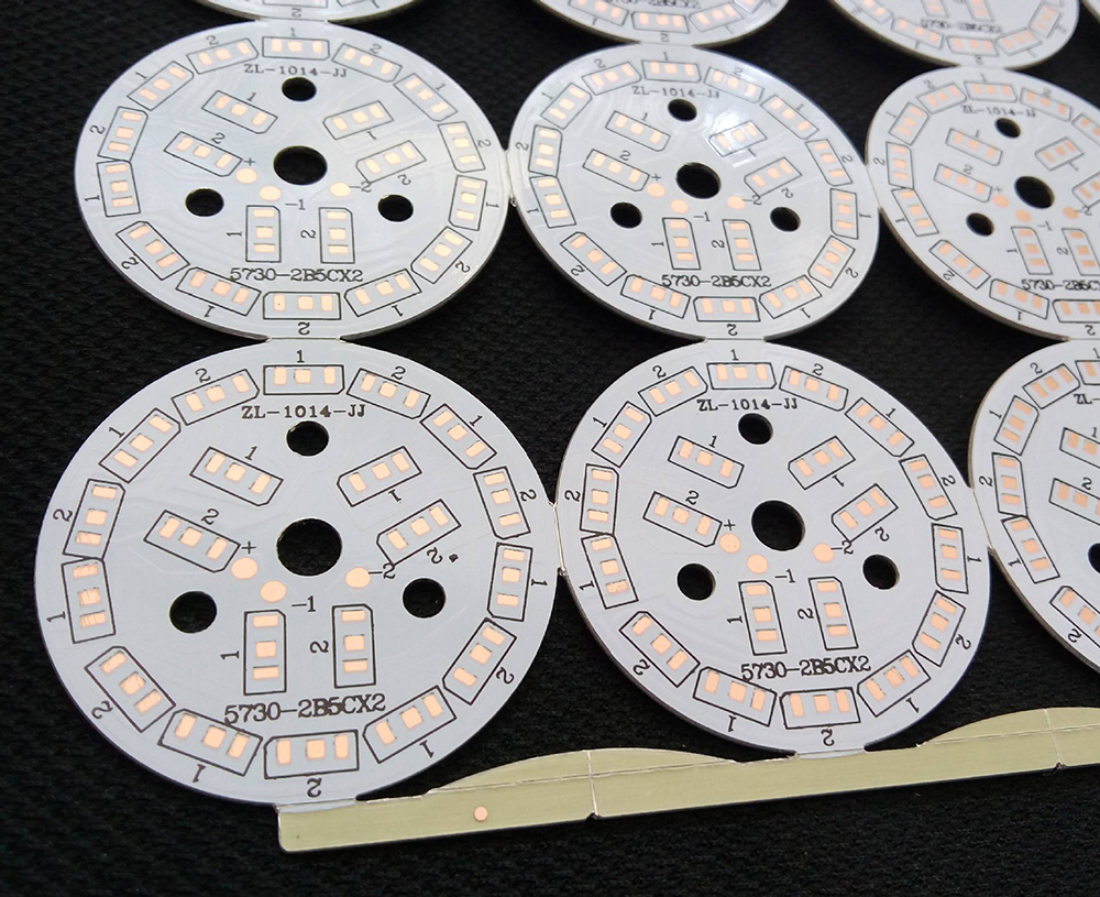
- LED light
- Smartphones and consumer electronics

- Communication equipment
- Automotive electronic systems
- Industrial control devices
- Medical electronic equipment
Recommended PCB Etching Machines
Modern PCB manufacturing lines use automated etching equipment to maintain consistent production quality. Industrial PCB etching machines typically include double-side spray systems, conveyor speed control, temperature regulation, and chemical concentration monitoring.
Advanced equipment ensures uniform copper removal and improves overall manufacturing efficiency.
Conclusion
PCB chemical etching remains one of the most important technologies in circuit board manufacturing. By removing unwanted copper in a controlled chemical process, manufacturers can create precise electronic circuits used in modern electronic products.
With the continued development of automated PCB etching machines and improved manufacturing technology, chemical etching will continue to play a vital role in electronics production.