High-Tolerance Etching for Bipolar Plates, Titanium Meshes, Speaker Grilles & More
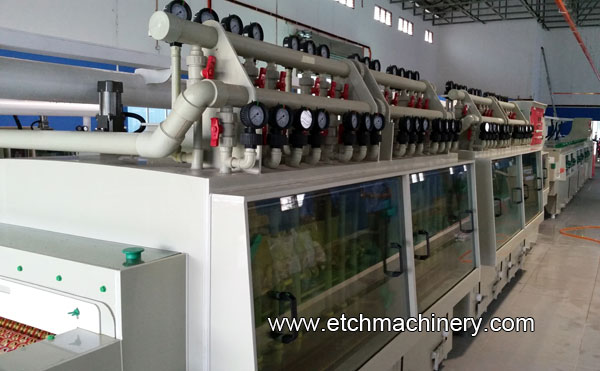
Stainless Steel Filter Mesh chemical milling Machine
Precision Photochemical Etching Solutions for Demanding Applications
Our advanced Double-Spray Stainless Steel Filter Mesh Chemical Milling Machine delivers unmatched precision (±0.02mm tolerance) for industrial photochemical etching processes. Designed for high-volume production, this system handles intricate etching of stainless steel, titanium, copper, and brass components ranging from 0.05mm to 2mm thickness.
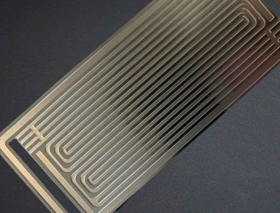
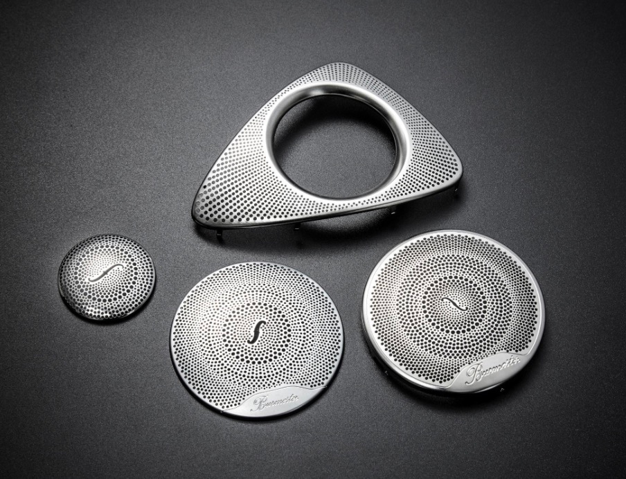
Features:This double spray precision Stainless Steel Filter Mesh Etching Machine is Photochemical etching machining equipments. It Can be chemical milling bipolar plate,titanium mesh for foldable screen smartphones,photo etched speaker grilles,TV shadow masks, Grids, shims, Washers, sieves, filter meshes, SMT, choppers, encoder, disks,speaker grills, EMI shieldingand so on.It mainly used on metal etching work.
Process flow: Load → Etching (8 meters)→ High pressure Rinsing→ City water Rinsing → suck dry→ Unload
Main technical parameter:
Power: 20kw/380V/50hz
Etching width: 650mm/1000mm/1220mm/1550mm (can be order)
Tolerance: ±0.02mm
Temperature: 0 to 65°C
Heater: 3KW,Titanium pipe
Cooling system: PE cooling system
Machining thickness: 0.05 to 2mm
Motor: 4KW*4sets
Etching system: Double spraying & Oscillate nozzles
Out size: 6550*1650*1550mm
Weight: 3500kg
Control system: Convey, Spray, Temperature, Pressure, Network filter
Application:this Stainless Steel Filter Mesh chemical milling Machine can be Photo etching process filter mesh,
Shims & spacers,
Metal encoder disk,
Drum Doctor Blade,
etched resistor,
Optical mask & air slit,
valve plate,
metal nameplate,
Step lids,
chemical etching material kinds,
toy model accessories,
Charge Corona Grid,
metal business card,
metal etching stencil,
Ground lug terminal,
PCB shielding/ copper PCB board,
Gift & Present & Specially designed,
Mesh & grid & filter
chemical milling process video
Applications
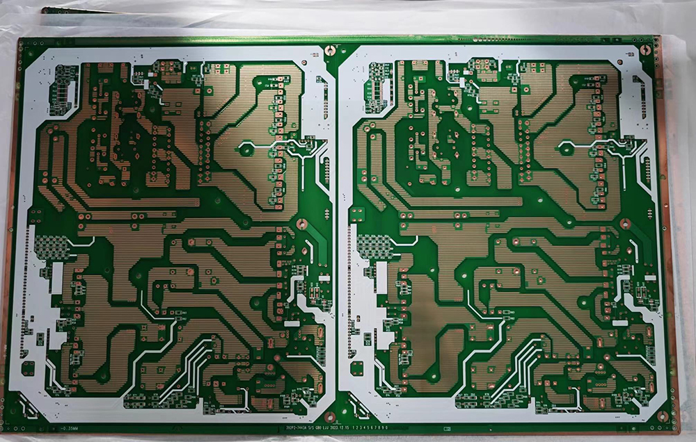
PCB Manufacturing
Ideal for solder mask application in high-density interconnect (HDI) PCBs
Fine-Line Circuits
Perfect for creating precise circuit patterns down to 2.0mil resolution
Multilayer Boards
Ensures perfect layer-to-layer registration for complex multilayer designs
High-Volume Chemical milling
Automated alignment reduces setup time and increases throughput
Etching machine application
PCB exposure
solder mask and circuit exposure
Bipolar Plates
High-tolerance etching for fuel cell components
High precision parts
photo chemcial etching mesh sample
Speaker Grilles
Aesthetic and functional components for audio devices
Why Choose Our Etching Machines?
✓
High precision etching down to 50μm for intricate patterns
✓
Double-side spray technology for uniform etching
✓
Chemical regeneration systems for reduced waste
✓
Adjustable spray pressure and temperature control
✓
Robust construction for corrosive industrial environments
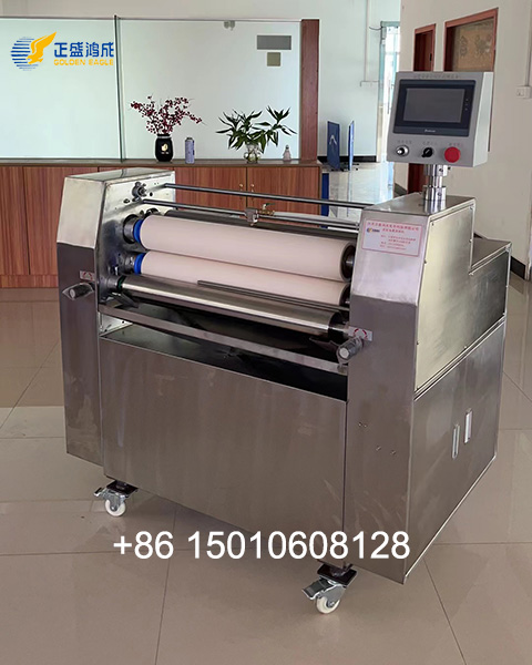
This machine is a roller-type photosensitive ink coating machine. You can use this machine to finish single side or double side coating work. Coating roller wheel surface with precision screw thread.
Circuit Production Capacity: 5-6 panels per minute
Solder Mask Production Capacity: 2-3 panels per minute
Dimensions: 2700×1630×1750mm
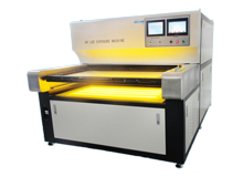
This double-sided UV LED exposure machine is engineered for mass production of various PCB types including dry film, wet film, inner layer and outer layer applications. Featuring advanced light uniformity technology and precise vacuum systems.
Applicable to: Dry Film/Wet Film & Photosensitive Ink Development.
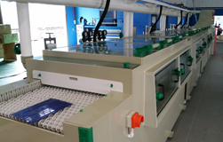
Machine process: Load → Developing → water washing → squeeze→cold & hot Drying → Unload
Machine dimension :8000*1700*1850mm
The Photoresist developing cleaning drying Machine can be built for use with all common aqueous resists, including: dry film photoresists, liquid resists, and dry film and liquid solder mask resist for PCB.
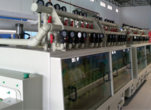
Machine process:Load → Etching1,2 → Etching3,4 → Pressure Washing → City Water Washing→ Checking →Stripping1,2 → Pressure Washing → City Water Washing → Blot Up → Cold & Hot Dry → Unload
The photo chemical Etching Line for PCB for double-sided or multi layer PCB or thin copper etching uses with high precision.
Chemical etching is a precision manufacturing process that uses chemical solutions to remove material selectively, creating complex and highly accurate parts. This technology is essential for producing printed circuit boards (PCBs) and precision metal components across various industries.
Key Features of Modern Etching Systems:
Today's advanced chemical etching machines incorporate precision spray nozzles, temperature-controlled solutions, and efficient waste management systems. Modern equipment offers uniform material removal, minimal chemical consumption, and high throughput. The most sophisticated systems feature automated conveyor speeds, solution concentration monitoring, and integrated quality control.
Applications of Chemical Etching:
PCB Manufacturing: Creating circuit patterns on copper-clad laminates
Metal Nameplates & Signage: Producing decorative and informational plates
Industrial Filters & Screens: Manufacturing precision meshes and sieves
Stamping & Cutting Dies: Preparing tools for manufacturing processes
Medical & Aerospace Components: Creating precision parts with complex geometries
What is the smallest aperture achievable by chemical etching?
Standard photochemical milling (PCM) achieves 25-50 μm apertures reliably on 0.10-0.20 mm sheet. With optimized process, fine-grain photoresist, and collimated UV, 10-15 μm apertures are achievable on thin nickel or stainless sheet (<0.10 mm). Below 10 μm, electroforming becomes the preferred method.
What tolerance can chemical etching achieve for filter mesh?
Standard tolerance: ±10% of nominal aperture, or ±5 μm (whichever is larger). For example, a 100 μm aperture has ±10 μm tolerance; a 50 μm aperture has ±5 μm tolerance. With tight process control, ±2 μm is achievable on thin sheet for critical applications.
Stainless steel vs copper vs nickel for filter mesh — which to choose?
Stainless steel (304/316L) is the most common — corrosion-resistant, durable, food-grade compatible. Copper is cheaper and easier to etch but oxidizes. Nickel is the premium choice for alkaline battery separators and hydrogen applications — expensive but stable at high temperature. Choose based on fluid compatibility, temperature, and cost.
What thickness of stainless steel for filter mesh?
Typical 0.10-0.50 mm. For aperture <50 μm, use 0.05-0.15 mm sheet. For 100-300 μm apertures, 0.20-0.40 mm. For coarse screens (>500 μm), 0.50-1.0 mm. Sheet thickness must be selected based on mechanical strength requirement of the application.
What is the difference between etching and electroforming for filter mesh?
Etching removes material from a solid sheet; electroforming builds up metal on a mandrel. Etching is faster, cheaper, and works on thicker sheets. Electroforming produces smoother walls and tighter tolerance on very fine apertures (5-25 μm). Choose etching for 25+ μm apertures and high-volume production; choose electroforming for ultra-fine mesh and small batches.
Can chemical etching produce 3D filter structures?
No. Chemical etching is 2D only — it produces through-holes or recesses. For 3D filter structures (graduated porosity, depth-graded mesh), use laser drilling followed by etching, or sintered mesh. For depth-graded mesh, multiple exposures with different photoresist thicknesses can create stepped etch depths.
How much does a precision filter mesh etching line cost?
Lab-scale: GE-FET500 from $5,000 USD. Small-batch: GE-S650 from $5,500 USD. Production: GE-SK9 wide-format from $9,800 USD (supports 650-2500 mm width). Complete photochemical milling line with artwork generation, exposure, etching, and inspection: $25,000-$80,000 USD.