
Beijing Golden Eagle GE-DI8563-100ZH12 semi-automatic solder mask LDI exposure machine: 14,000 dpi resolution (±2μm precision), 12 DI lenses, 1,632 W hybrid-wavelength laser, ±12μm alignment, 5-6 p...
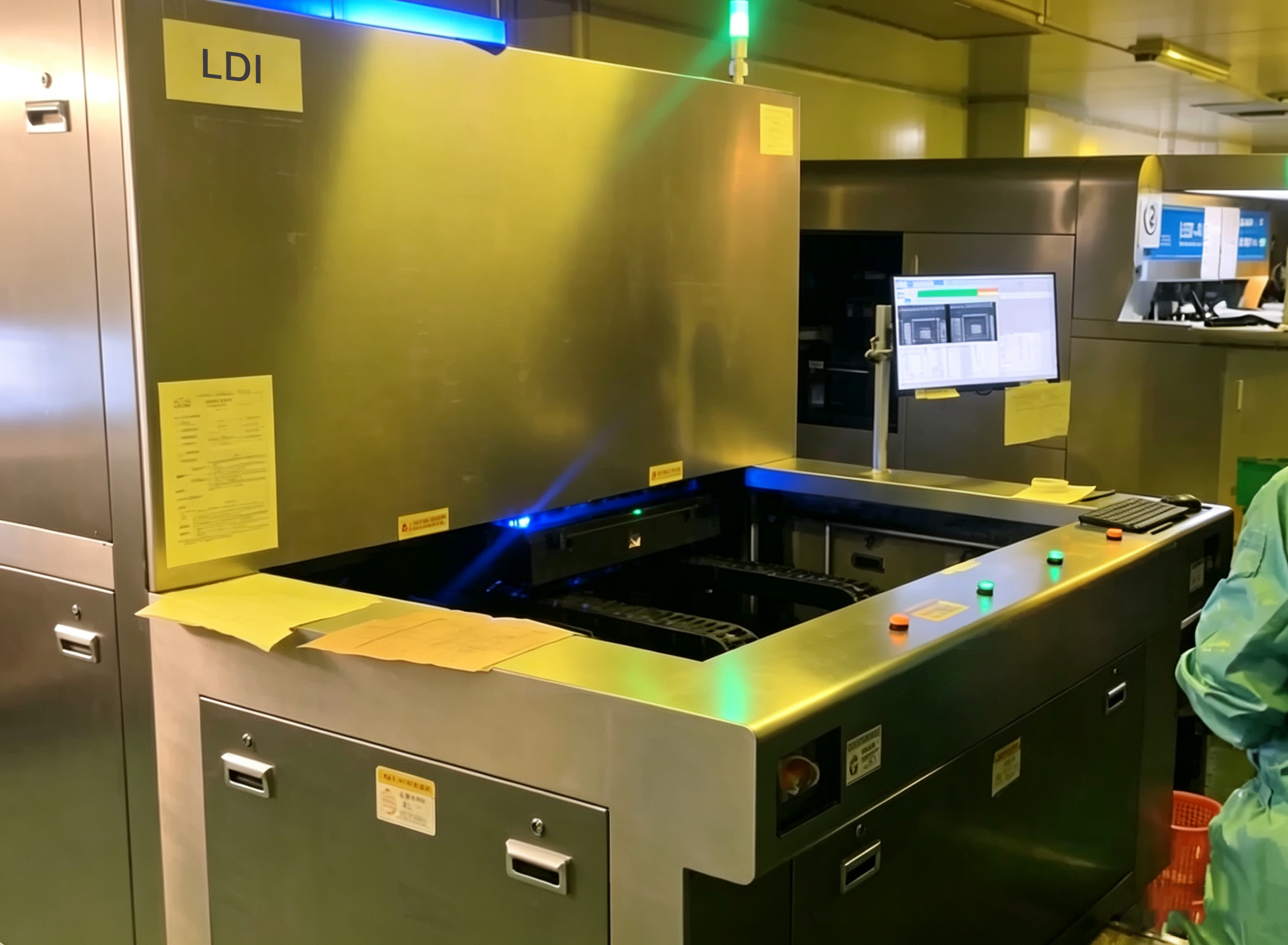
14,000 dpi semi-automatic Laser Direct Imaging — 12 DI lenses, ±2μm precision, 1,632 W hybrid laser
See the GE-DI8563-100ZH12 semi-automatic solder mask LDI (Laser Direct Imaging) exposure machine in real production: 12 DI lenses with hybrid-wavelength UV laser (1,632 W total) directly write solder mask patterns onto PCB panels, replacing traditional film exposure. Watch how 14,000 dpi resolution, ±2μm precision, and 4-mode scaling deliver stable high-yield solder mask imaging for HDI and fine-line PCB.
Subscribe to the Beijing Golden Eagle YouTube channel for more PCB equipment working videos.
LDI (Laser Direct Imaging) is the next-generation photolithography process for PCB manufacturing. Instead of using a glass phototool film to transfer the circuit image, a computer-controlled multi-lens laser array writes the pattern directly onto the photoresist. This removes the film cost, eliminates film-distortion errors, and enables line/space resolution down to 75μm (bridge) / 100μm (opening) — essential for fine-pitch solder mask, HDI, and 5G substrate production.
The Beijing Golden Eagle GE-DI8563-100ZH12 is a semi-automatic LDI exposure machine optimized for solder mask exposure on PCB panels from 300×300 mm to 630×830 mm, with 12 DI lenses in parallel scanning, ±2μm data precision, ±12μm alignment, and inline throughput of 5-6 panels per minute.
Optical data resolution of 14,000 dpi (approximately 1.81μm per pixel) with ±2μm positioning precision and ±10% line width uniformity. Bridge > 75μm and opening > 100μm at 25μm solder mask thickness.
Front-side target alignment with ±12μm layer-to-layer registration accuracy. ±350μm depth of focus tolerates substrate warp and thickness variation for high-yield imaging.
12 parallel DI lenses with hybrid-wavelength UV laser source. 136 W per head (1,632 W total) and ≥95% illumination uniformity. Multi-zone exposure saves laser power on sparse-pattern boards.
Direct writing from Gerber 274X / 274D or ODB++ files eliminates phototool film cost, film storage, and rework caused by film distortion — lower per-panel cost for fine-pitch solder mask.
Single-machine cycle time 10 seconds/side at 500 mJ/cm². Inline throughput of 5.0-6.0 panels/min on 24.5″×32.5″ (630×825.5 mm) panels — suitable for medium-to-high volume solder mask lines.
4 scaling modes (Fixed / Auto / Zone / Measured) for precise compensation of substrate expansion. Built-in 2D barcode reader logs date, time, serial number and scaling factor for full production traceability.
Source: Beijing Golden Eagle official specification sheet. Specifications subject to confirmation per customer application.
| Model 型号 | GE-DI8563-100ZH12 (Semi-Automatic Solder Mask LDI Exposure Machine) |
|---|---|
| Production Size 生产尺寸 | Min: 12″ × 12″ (300 × 300 mm) | Max: 24.5″ × 32.5″ (630 × 830 mm) |
| Substrate Thickness 基材厚度 | 0.1 mm – 6.0 mm |
| Bridge / Opening 桥 / 开窗尺寸 | Bridge > 75 μm | Solder mask opening > 100 μm (at 25 μm dry film thickness) |
| Data Resolution 数据解析力 | 14,000 dpi (approx. 1.81 μm per pixel) |
| Positioning Precision 数据解析精度 | ± 2 μm |
| Line Width Uniformity 线宽均匀性 | ± 10% (across exposure area) |
| Depth of Focus 景深 | ± 350 μm |
| Alignment Accuracy 对位精度 | ± 12 μm (front-side target alignment) |
| Single-Machine Throughput 单机产能 | 10 ± 1 sec / side @ 500 mJ/cm² (24.5″×32.5″ / 630 × 825.5 mm panel) |
| Inline Throughput 自动线产能 | 5.0 – 6.0 panels / minute (24.5″×32.5″ / 630 × 825.5 mm panel @ 500 mJ/cm²) |
| Photoresist 感光材料 | Conventional solder mask ink / DI-specific ink (liquid photoimageable solder mask) |
| DI Lens Count DI 镜头数 | 12 lenses (multi-beam parallel scanning) |
| Illumination Uniformity 均匀性 | ≥ 95% (across exposure area) |
| Laser Wavelength 激光波长 | Mixed wavelength (UV), matched to solder mask sensitivity |
| Laser Power 激光功率 | 136 W per head × 12 heads = 1,632 W total |
| Exposure Mode 曝光方式 | Single-sided exposure (top side) |
| Data Input 资料输入 | Gerber 274X | Gerber 274D | ODB++ |
| Scaling Management 图形胀缩管理 | 4 modes: Fixed / Auto / Zone / Measured |
| Mark Scanning 扫码 MARK | 2D barcode reader: date, time, serial number, scaling factor etc. |
| Target Alignment 靶标对位 | Front-side alignment |
| Multi-Zone Exposure 多区域曝光 | Supported (saves laser power on sparse patterns) |
| Working Height 工作高度 | 950 ± 50 mm (operator-ergonomic level) |
| Working Environment 工作环境 | 22 ± 2 °C | 55 ± 5% RH | Class 10,000 cleanroom, yellow-light room required |
| Power Supply 电源需求 | 3-phase 5-wire | 380 VAC | 50 Hz | 30 KVA |
| Compressed Air 气压源 | 6 – 7 kg/cm² | 500 L/min | clean dry air |
| Chilled Water 冰水需求 | 7 – 12 °C | 70 L/min | 2 – 3 kg/cm² (2 circuits for laser cooling) |
| Machine Dimensions 设备尺寸 (L × W × H) | 3,100 × 1,850 × 2,290 mm (excludes chiller & cooling unit) |
| Net Weight 设备重量 | Approx. 4,500 kg (total) |
14,000 dpi resolution and ±2μm precision support the fine line/space required for high-density interconnect boards used in smartphones, wearables, and IoT devices.
±12μm alignment and automatic expansion/contraction compensation deliver consistent registration across 4- to 24-layer boards.
50μm solder dam and 80μm opening capability meet the solder mask requirements of fine-pitch BGA, QFN, and 0201 components.
Fine-line imaging suitable for 5G communication boards, IC substrates, and chip-on-board applications.
Direct Gerber import — perfect for prototype shops and small-batch fabs switching between product designs without film changeover.
Drop-in replacement for traditional film exposure lines, with no film storage, no film distortion, and lower per-panel cost.
| Item | Traditional UV + Film | GE-DI8563-100ZH12 LDI |
|---|---|---|
| Phototool required | Yes (silver halide film) | No — direct from Gerber / ODB++ |
| Optical resolution | 50-75 μm (limited by film) | 14,000 dpi (approx. 1.81 μm per pixel) |
| Solder mask bridge | 100-150 μm (film distortion) | > 75 μm |
| Solder mask opening | 150-200 μm | > 100 μm (at 25 μm dry film thickness) |
| Alignment accuracy | ±25-50 μm (film distortion) | ± 12 μm |
| Positioning precision | N/A | ± 2 μm |
| Product changeover | New film required | Load new Gerber / ODB++ — seconds |
| Recurring consumable | Phototool film + developer | None (laser only) |
| Throughput (630×825.5 mm) | 1-2 panels / min (film alignment) | 5.0 – 6.0 panels / min (12-lens parallel) |
| Best for | Low-cost, low-precision production | Fine-pitch solder mask, HDI, 5G substrate, high-volume |
LDI (Laser Direct Imaging) is a photolithography technology that uses computer-controlled laser beams to directly write circuit patterns onto photoresist-coated PCBs, eliminating the need for physical phototools/films. LDI delivers higher alignment accuracy, finer line/space resolution, and faster changeover between product designs. The GE-DI8563-100ZH12 uses 12 DI lenses in parallel to achieve very high throughput.
Traditional UV exposure uses a glass phototool (film) with the circuit pattern, which is aligned and pressed against the photoresist. LDI removes the film step: a digital Gerber / ODB++ file drives a multi-lens laser array that scans the pattern directly. Benefits of LDI: no film cost, no film distortion, no alignment drift from film handling, finer resolution (14,000 dpi / 1.81μm on the GE-DI8563-100ZH12), faster product changeover, and better registration between layers.
The GE-DI8563-100ZH12 is optimized for solder mask exposure on PCB panels from 300×300 mm to 630×830 mm and substrate thickness from 0.1 mm to 6.0 mm. It is suitable for fine-pitch BGA/QFN/0201 components, HDI boards, 5G communication boards, IC substrates, and chip-on-board production. The 12-lens parallel scanning delivers 5-6 panels per minute inline throughput.
Optical data resolution is 14,000 dpi (approx. 1.81μm per pixel) with positioning precision of ± 2μm and line width uniformity of ± 10% across the exposure area. The minimum achievable bridge is > 75μm and opening is > 100μm at 25μm dry film thickness. Alignment accuracy is ± 12μm with ± 350μm depth of focus to tolerate substrate warp.
The GE-DI8563-100ZH12 uses 12 DI lenses with parallel scanning. Each head is 136 W, total optical power is 1,632 W. Illumination uniformity across the exposure area is ≥ 95%. Multi-zone exposure is supported to save laser power on sparse-pattern boards.
Single-machine cycle time is 10 seconds per side at 500 mJ/cm² on a 24.5″×32.5″ (630×825.5 mm) panel. Inline throughput with automatic loading reaches 5.0 - 6.0 panels per minute. Throughput depends on the solder mask sensitivity, panel size, and the number of alignment targets.
The GE-DI8563-100ZH12 must be installed in a yellow-light room with Class 10,000 cleanroom conditions, ambient temperature 22 ± 2 °C, and relative humidity 55 ± 5%. Power supply is 3-phase 5-wire / 380 VAC / 50 Hz / 30 KVA. Compressed air 6-7 kg/cm² at 500 L/min. Chilled water 7-12 °C at 70 L/min, 2-3 kg/cm², 2 circuits. Beijing Golden Eagle provides on-site installation, cleanroom guidance, and operator training.
The GE-DI8563-100ZH12 supports Gerber 274X, Gerber 274D, and ODB++. It also supports 4-mode scaling management (Fixed, Auto, Zone, Measured) for precise compensation of substrate expansion. The built-in 2D barcode reader logs production data (date, time, serial number, scaling factor) for full traceability.


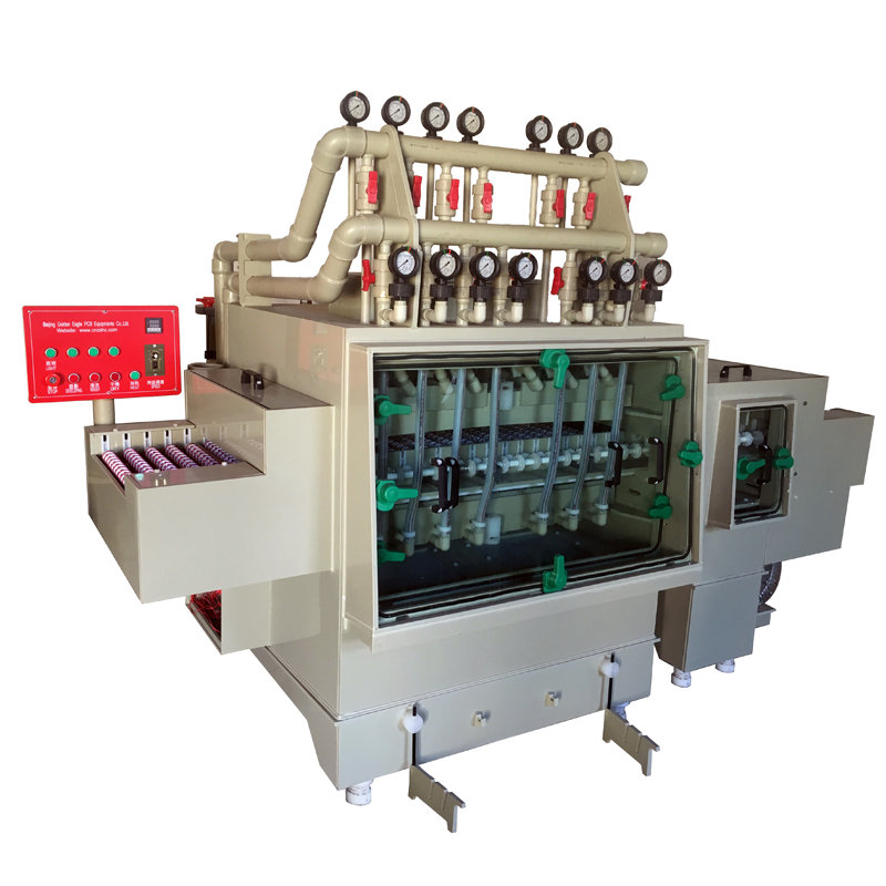
Pair this LDI direct-imaging exposure machine with our PCB developing machine (GE-XY650 or GE-D650W) for the wet stage downstream. The GE-XY650 includes developing + pressure wash + cold/hot drying in a single inline unit (8 m machine length, 28 kW).