
YB-800 two-component liquid photosensitive solder-resist ink for PCB. 3 mil green-oil bridge control, BGA via plugging, lead-free HASL, ENIG and immersion tin. RoHS standard, halogen-free variant a...
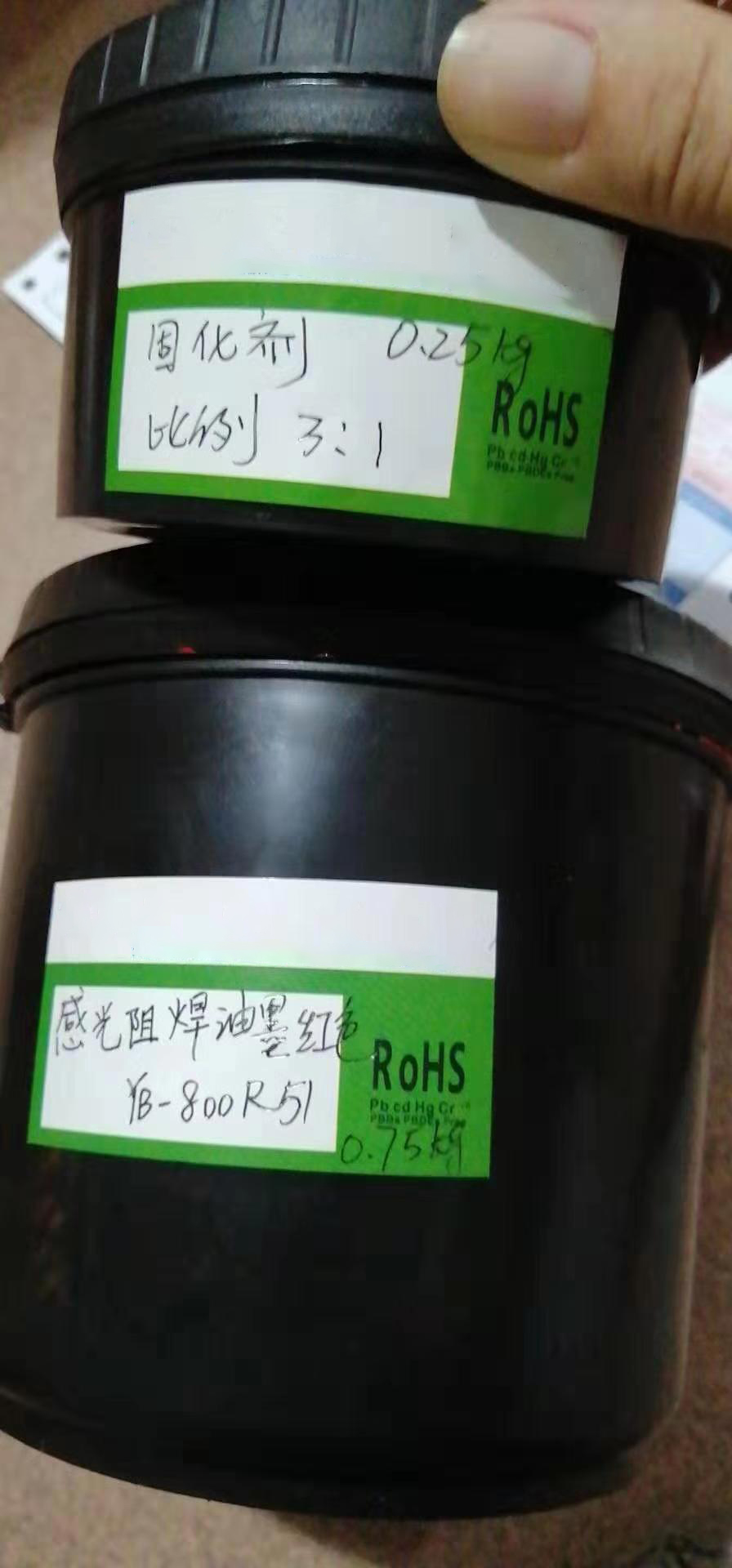
A two-component liquid photosensitive solder-mask ink for fine-line PCB. 3 mil green-oil bridge control, BGA via plugging, full compatibility with lead-free hot-air leveling, ENIG and immersion tin plating. Standard grade meets EU RoHS; halogen-free variant on request.
YB-800 is a two-component liquid photosensitive solder-mask ink for fine-line printed circuit boards. It is mixed 3 : 1 (base : hardener) by weight, screen-printed, pre-baked, exposed through a phototool on a 21-step exposure scale, developed in 1% sodium carbonate, and post-cured. The cured film gives a hard, glossy green solder mask that survives lead-free hot-air leveling, ENIG plating and immersion tin plating without lift, blister or chemical attack.
The standard grade is formulated to meet EU RoHS requirements. For customers who need a halogen-free solder mask, the same YB-800 is available in a halogen-free variant. YB-800 is one of the workhorse liquid photoimageable solder masks used in the Chinese PCB industry and is the right choice for multilayer and fine-line boards where 3 mil (75 µm) green-oil bridges and BGA via plugging are routine.
The full sequence from substrate to finished part. Exact temperatures and times depend on the application; full details are in the operating parameters table below.
| Item | Specification |
|---|---|
| Type | Two-component liquid photosensitive solder mask |
| Color | Green (standard) |
| Mixing ratio | 3 : 1 base : hardener (by weight) |
| Thinner | Supplier-recommended YB thinner or PGMEA |
| Mesh (standard PCB) | 43T polyester |
| Mesh (lead-free / ENIG / immersion tin) | 36T polyester |
| Pre-bake (first side) | 75 °C × 15–20 min (hot-air) |
| Pre-bake (second side) | 75 °C × 25–30 min (hot-air) |
| Exposure | 21-step scale, 9–13 grid sensitivity |
| Developer | 1 wt% Na2CO3 aqueous |
| Develop pressure | 2.0–2.5 kg/cm² |
| Develop temperature | 30 ± 2 °C |
| Develop time | 40–90 seconds |
| Post-cure (HASL) | 150 °C × 60 min |
| Post-cure (ENIG / immersion tin) | 150 °C × 50 min |
| Post-cure (via plug, two-stage) | 75 °C × 120 min, then 150 °C × 60 min |
| Green-oil bridge | 3 mil (75 µm) |
| Compatibility | Lead-free HASL, ENIG, immersion tin, BGA via plug |
| Compliance | EU RoHS standard; halogen-free variant available |
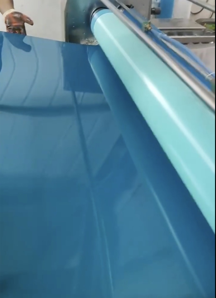
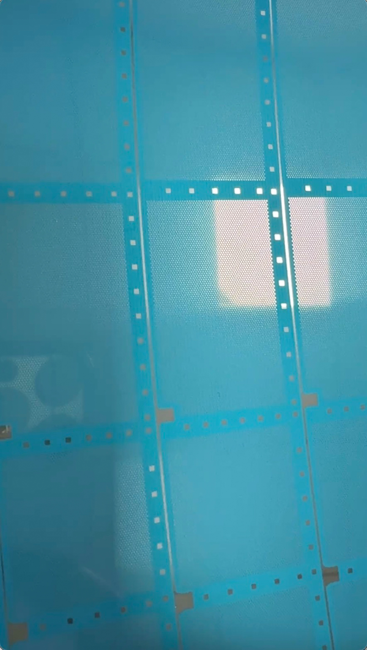
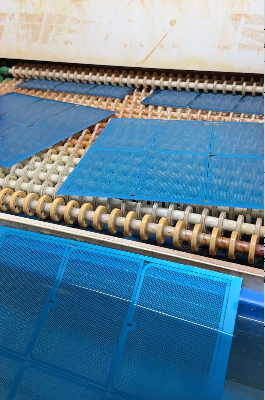
Each batch is checked on a production test panel before it ships. Below: typical adhesion, exposure and development results on PCB and metal substrates.
Send us your substrate, panel size and process. We will send a small sample for trial and a quotation for production volumes.
Dry film solder mask is a laminated sheet that is hot-roll laminated, exposed and developed. It gives very consistent thickness but is limited in how thick a film it can produce and how well it conforms to surface topography. YB-800 is a liquid that is screen-printed, pre-baked, exposed and developed. It can be applied thicker, conforms to topography better, and is the standard for BGA via plugging and modern fine-pitch PCB.
Yes. YB-800 is formulated for BGA via plugging. Use the two-stage post-cure (75 °C × 120 min, then 150 °C × 60 min) for plugged-via boards to make sure the ink in the via fully cures without voids.
3 mil (75 µm) on a properly tuned line. Use the 43T mesh for standard PCB, the 36T mesh for lead-free / ENIG / immersion tin boards (the thicker deposit helps the mask survive the plating bath).
Yes. The same YB-800 chemistry is available in a halogen-free variant. Specify "halogen-free" when ordering, and we will quote and supply the matching grade.
Yes, but use the supplier-recommended thinner only. YB thinner or PGMEA at the recommended addition rate. Off-the-shelf generic thinners can leave a film that interferes with the photo reaction, causes scumming, or reduces the cured film properties.