


PCB Exposure Technology Explained
PCB exposure machines are essential equipment in the printed circuit board manufacturing process. Using UV light technology, these machines transfer circuit patterns from photomasks onto photosensitive-coated boards. The precision of this process directly impacts the quality and functionality of the final PCB.
Key Features of Modern Exposure Systems:
Today's advanced exposure machines incorporate UV LED technology that offers significant advantages over traditional mercury vapor lamps. LED systems provide consistent light output, longer lifespan (up to 20,000 hours), reduced energy consumption (up to 70% less), and instant on/off capability. The most sophisticated machines feature CCD automatic alignment systems that ensure perfect registration between layers, critical for multi-layer PCB production.
Applications in PCB Manufacturing:
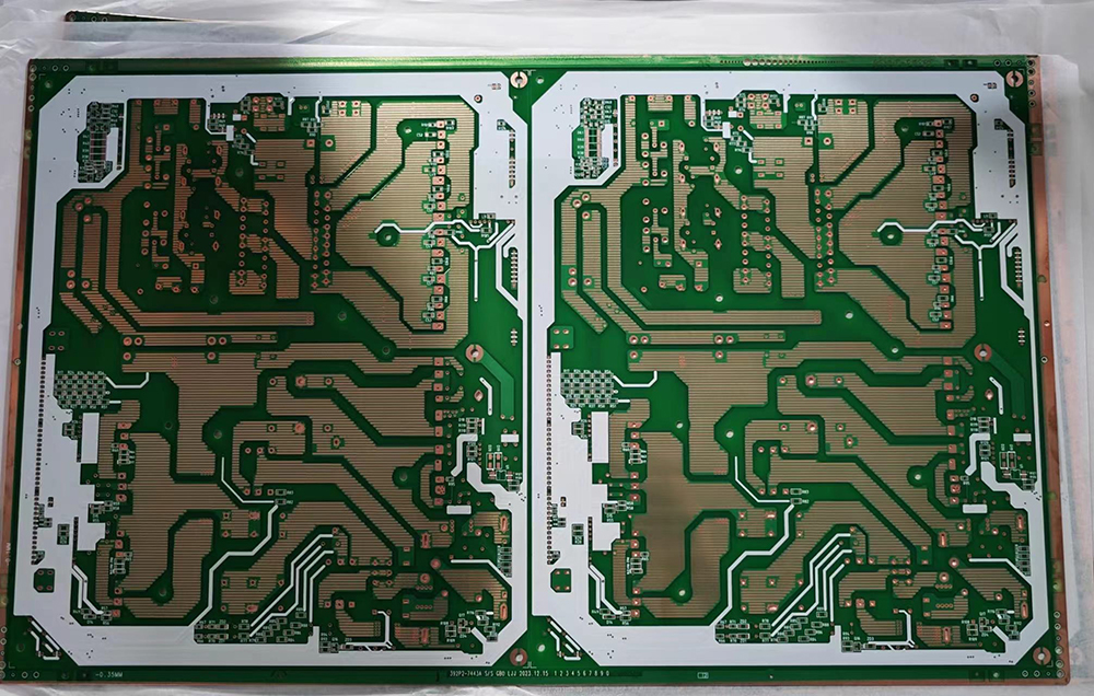
- Inner Layer Processing: Creating circuit patterns on individual PCB layers with precision up to 50μm
- Outer Layer Imaging: Transferring patterns to outer copper layers with ±5μm accuracy
- Solder Mask Application: Applying protective coatings with precise openings for components
- Legend Printing: Adding component identification markings with high resolution
- Flexible Circuits: Specialized exposure for flexible PCB materials requiring specific wavelength control
Applications in Metal etching & printing:
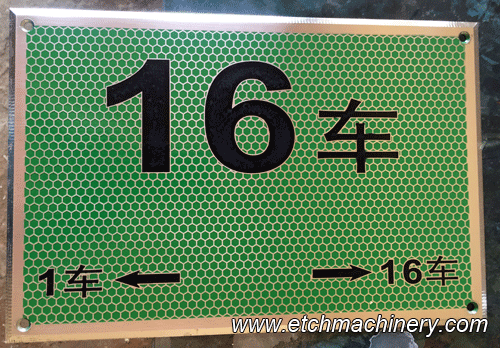
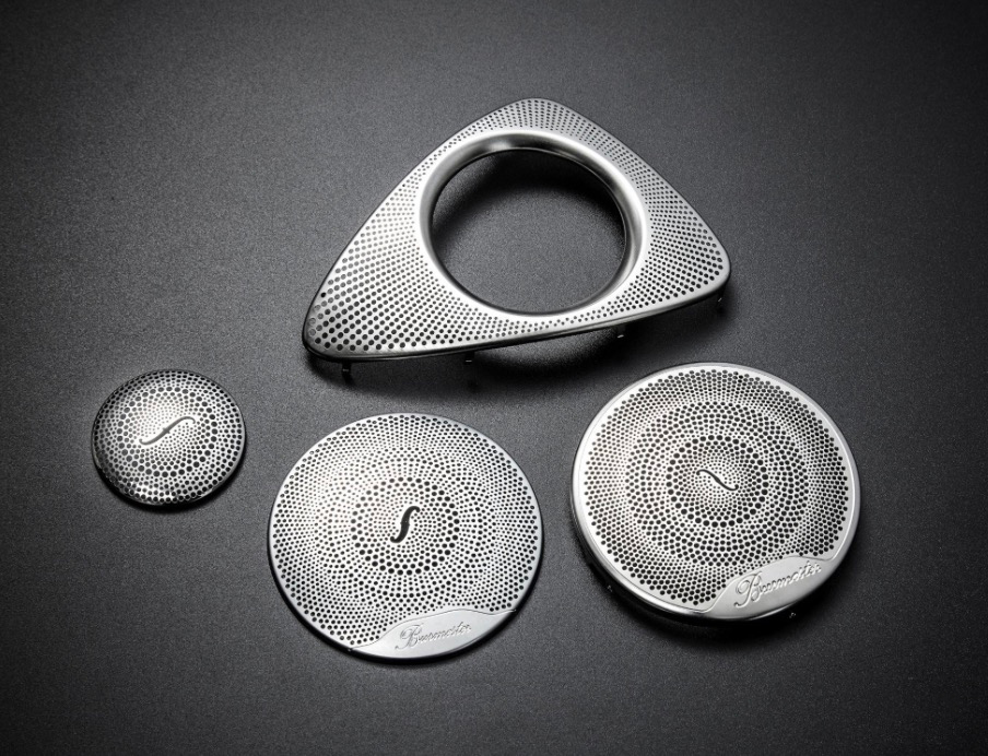
- Decorative Surface Patterning: Transfers intricate designs onto jewelry, cutlery, and luxury goods through photoresist exposure before acid etching.
- Artistic Metalwork: Projects detailed artwork onto copper, brass, or silver sheets for sculptures and architectural elements.
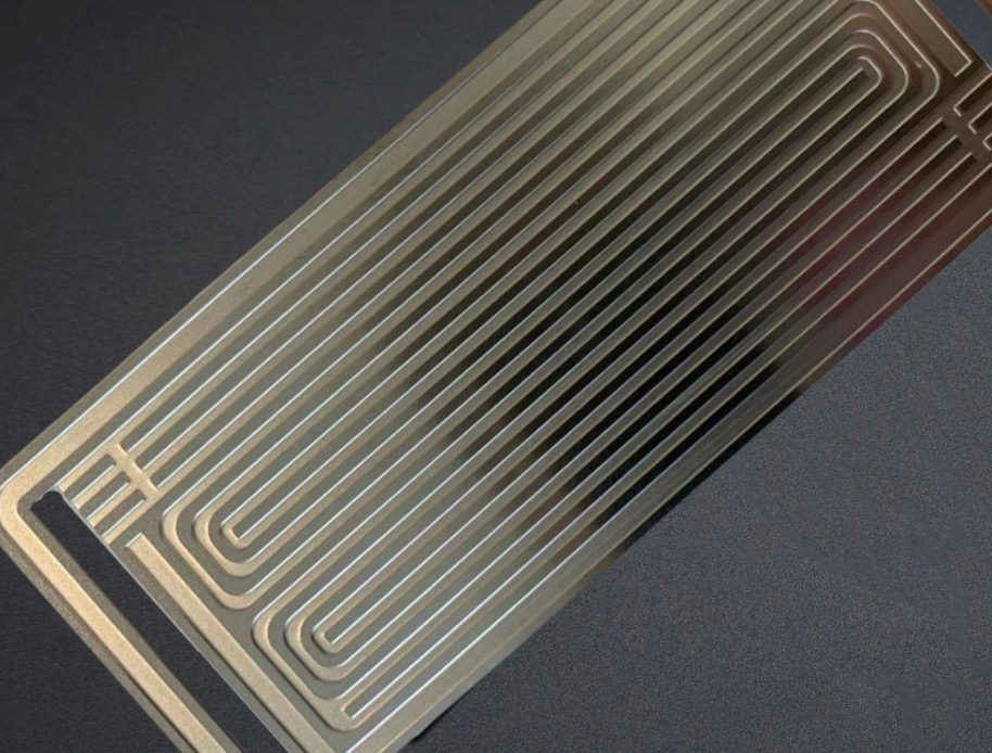
- Precision Component Manufacturing: ACreates micro-patterns on surgical tools, aerospace parts, and watch components for functional etching.
- filter mesh: Creates micro-patterns on metal sheet double side with high resolution.