PCB Developing Technology Explained
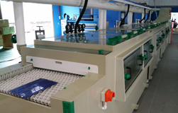
PCB developing machines are essential equipment in the printed circuit board manufacturing process. Using precise spray technology, these machines remove unexposed photoresist after the exposure process, revealing the circuit pattern. The accuracy and consistency of this process directly impact the quality of the final PCB.
Key Features of Modern Developing Systems:
Today's advanced developing machines incorporate precision spray nozzles, temperature-controlled solutions, and efficient drying systems. Modern machines offer uniform development, minimal chemical consumption, and high throughput. The most sophisticated systems feature automated conveyor speeds, solution concentration monitoring, and integrated quality control.
Applications in PCB Manufacturing:
- Inner Layer Processing: Developing circuit patterns on individual PCB layers
- Outer Layer Imaging: Developing patterns on outer copper layers
- Solder Mask Application: Developing solder mask patterns with precise openings
- Fine Line Circuits: High-precision development for HDI and advanced PCBs
- Flexible Circuits: Specialized development for flexible PCB materials
Applications in metal etching:
- Precision Pattern Transfer: Develops exposed photoresist to reveal intricate designs on jewelry, decorative items, and industrial components before acid etching.
- Industrial Marking & Labeling: Transfers logos, serial numbers, and safety markings onto metal surfaces for tools, machinery, and equipment plates.
- Artistic Metalwork: Develops complex patterns on copper, brass, and silver sheets for handmade crafts, sculptures, and architectural elements.
- Tool & Mold Manufacturing: Develops micro-patterns on cutting dies and embossing tools for leather, textiles, and packaging industries.


