Professional PCB Plating Solutions | Electroless Copper Plating Machines, Copper Electroplating Equipment & Tin Plating Systems
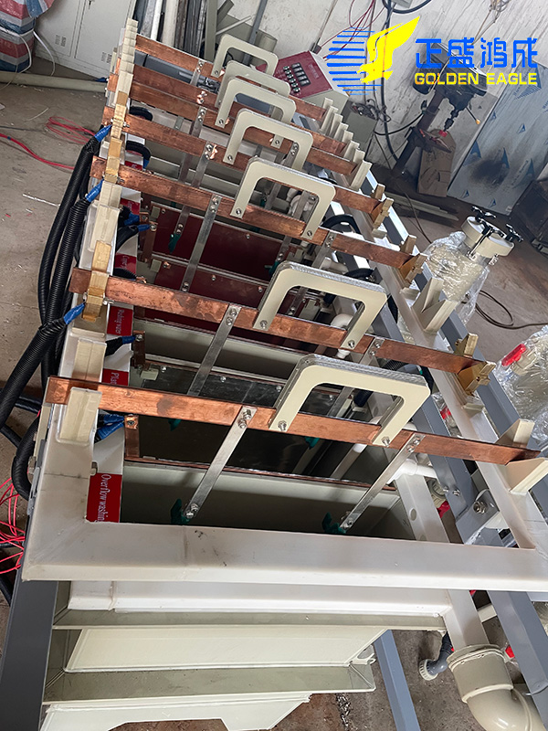
Advanced plating systems form the critical foundation for reliable PCB conductivity and solderability, enabling precise metallic layer deposition through chemical and electrochemical processes. These automated solutions deliver micron-level uniformity for hole wall coverage, surface finishes, and circuit formation across rigid, flex, and HDI boards serving automotive, aerospace, and 5G communication industries.
Key Features of Modern Plating Systems:
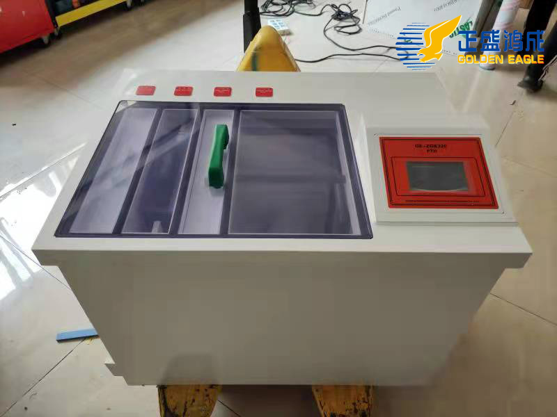
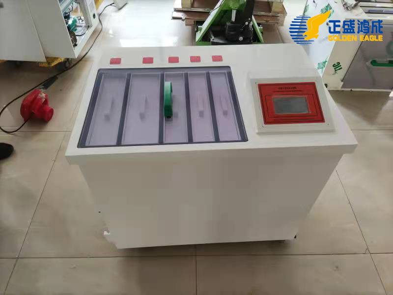
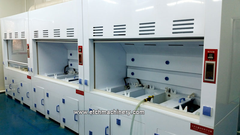
- Multi-Stage Process Control: Integrated tanks for degreasing, activation, acceleration, and plating with real-time chemical parameter monitoring
- Pulse Reverse Electroplating: Precision copper deposition with optimized throwing power for high-aspect ratio vias (>15:1)
- Selective Plating Technology: Programmable anode arrays and masking for zone-specific deposition thickness control (±0.1μm)
- Automated Chemical Management: Closed-loop dosing systems maintaining bath composition within 5% tolerance
- Environmental Compliance: Zero-discharge rinse water recycling and effluent treatment systems
- Smart Analytics Integration: IoT-enabled performance tracking with predictive maintenance alerts
Applications in PCB Manufacturing:
- Electroless Copper Deposition: Create uniform conductive layers (0.3-5μm) on non-conductive substrates for through-hole metallization prior to electroplating, ensuring reliable hole wall connectivity in multilayer boards.
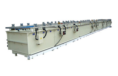
- Copper Electroplating Systems: Build conductive traces and increase copper thickness (up to 100μm) with superior throwing power for high-frequency circuits, supporting controlled impedance requirements in 5G/RF applications.
- Solderable Tin Finishing: Apply oxidation-resistant tin coatings (3-15μm) as final surface finish for component soldering, enabling high-reliability interconnections in automotive control modules.
- HDI Microvia Metallization: Achieve uniform copper deposition in laser-drilled microvias (<100μm diameter) through optimized agitation and pulse plating for next-generation wearable electronics.
- Custom Plating Solutions: Tailored configurations for specialty applications including thick-copper power boards (400+ μm), reel-to-reel flex circuit plating, and embedded component encapsulation.

_plating_machine_for_PCB.jpg)
_machine.jpg)
