LED UV Cold Light Source
Advanced 365-420nm LED technology provides consistent UV output without heat damage to sensitive PCB components, ensuring precise pattern transfer quality.

Professional UV LED exposure unit for screen making & stencil exposure with integrated drying cabinet

Features: The UV LED Exposure Unit for Screen Printing (GE-LED1200) is a complete screen making solution combining high-intensity UV LED exposure and an integrated drying cabinet. Perfect for screen printing stencil exposure, large-format graphics, textile screen printing, glass & ceramic decoration, and industrial screen making. The 365-420nm cold light source ensures fast, consistent exposure without heat damage to emulsions or mesh tension.
1、 Single band, high photoelectric conversion rate, uniform irradiation energy
UVLED exposure machine is a parallel light source, emitting 365nm / 395nm single band light source, no clutter energy consumption, energy uniformity can reach 90%, suitable for the use of precision route industry.
2、 High efficiency and energy saving:
UVLED uses ultraviolet diode chip to light up, which can light up instantly. The output energy can be set by itself, which is very energy-saving and easy to operate.
3、 No harmful substances discharged, safety and environmental protection:
UVLED exposure machine is a kind of UV light emitting diode chip, which is the conversion of electric energy to light energy. There is no pollution. It is a cleaner and more environmentally friendly curing method.
4、 Long service life, no consumables:
UVLED exposure lamp can be used for more than 20000 hours, and a UVLED curing light source can be used for several years.
Main technical parameter:
| Model Number | GE-LED1200 |
|---|---|
| Working Area (Table Size) | 1300 × 1600 mm |
| Light Source | 365-420nm LED UV Cold Light Source |
| Power Consumption | 1 KW |
| Voltage | 220V / 50Hz |
| Vacuum System | Integrated Vacuum Pressure System |
| Light Characteristics | Excellent stability, uniform illumination |
| Service Life | Long service life LED technology |
| Applications | PCB photolithography, solder mask exposure, pattern transfer |
| Workflow | Automated exposure and curing in single system |
Ideal for solder mask application in high-density interconnect (HDI) PCBs
Perfect for creating precise circuit patterns down to 2.0mil resolution
Ensures perfect layer-to-layer registration for complex multilayer designs
Automated alignment reduces setup time and increases throughput
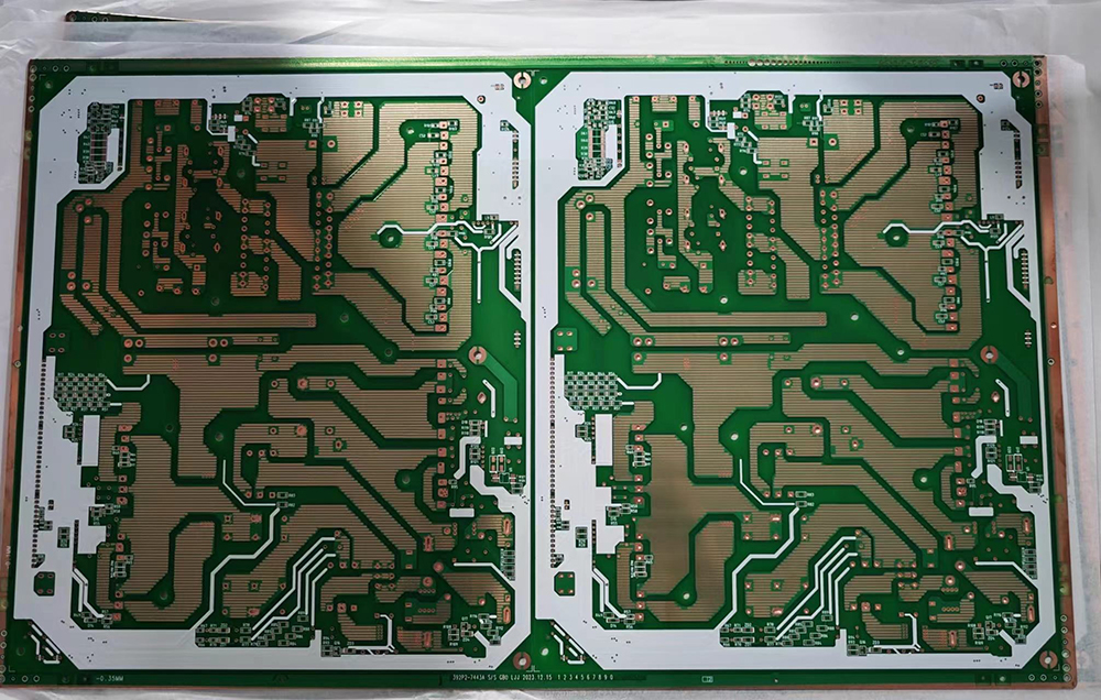
solder mask and circuit exposure
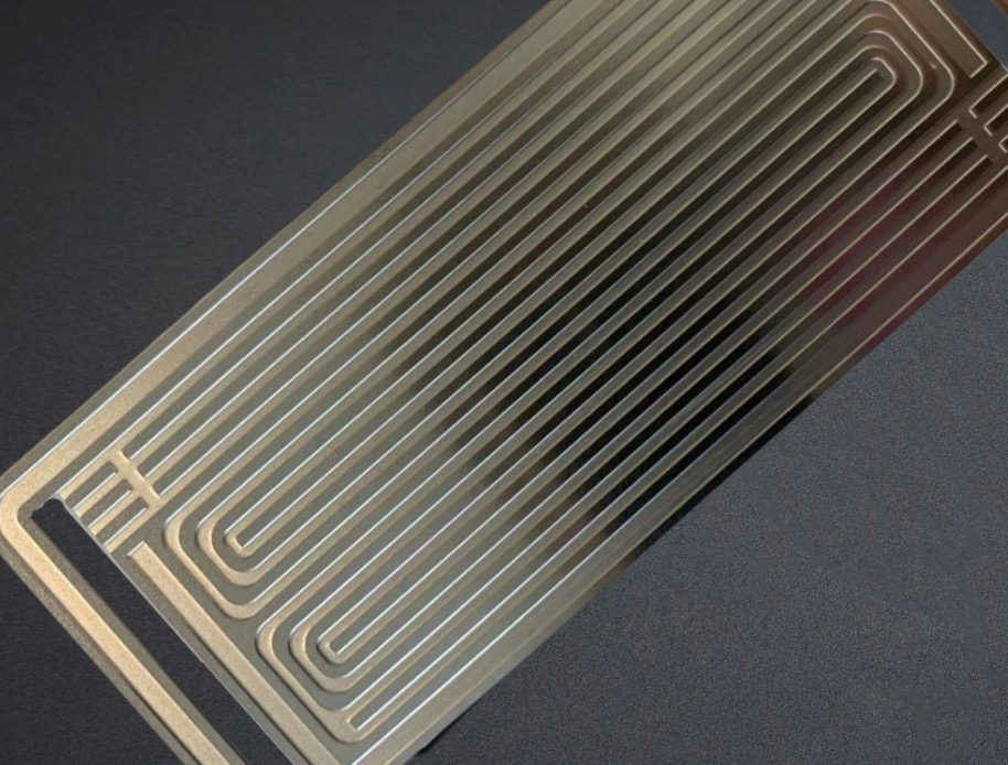
High-tolerance etching for fuel cell components

For foldable screen smartphones and advanced displays
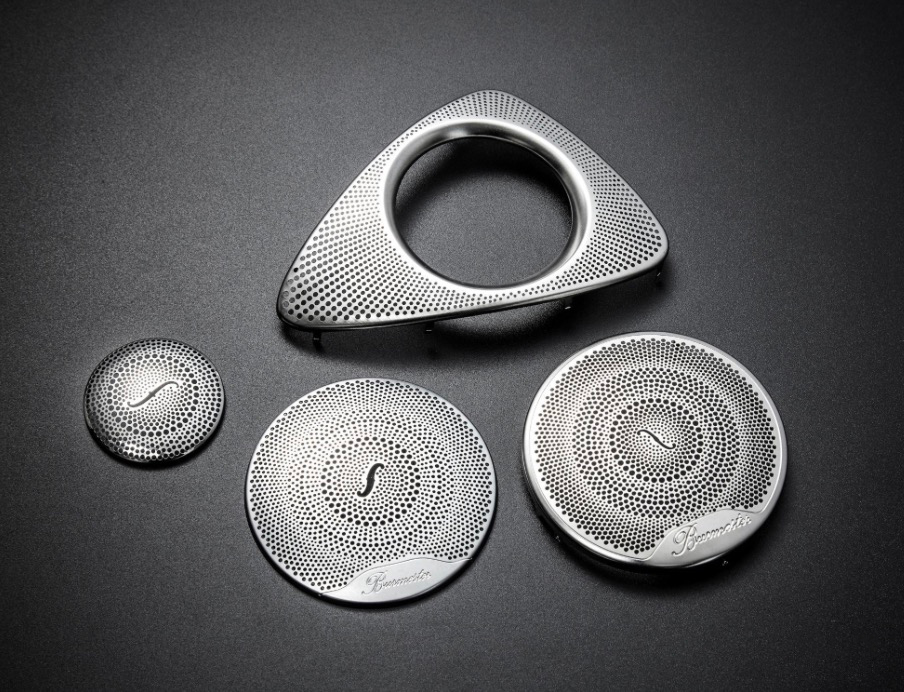
Aesthetic and functional components for audio devices
Advanced 365-420nm LED technology provides consistent UV output without heat damage to sensitive PCB components, ensuring precise pattern transfer quality.
Advanced optical system delivers perfectly uniform illumination across the entire 1300×1600mm working area, eliminating overexposure and underexposure issues.
Built-in vacuum pressure system ensures complete contact between the artwork film and PCB surface for razor-sharp pattern definition.
Only 1KW power consumption significantly reduces operating costs while maintaining professional-grade exposure quality and speed.
LED technology provides thousands of hours of maintenance-free operation compared to traditional mercury lamp systems that require frequent replacement.
Combines exposure and drying functions in a single automated system, streamlining PCB manufacturing workflow and reducing production time.
LED UV exposure offers several advantages: instant on/off operation (no warm-up time), consistent light output throughout its lifespan, significantly lower energy consumption, no harmful mercury content, and minimal heat generation that can damage sensitive boards. The 365-420nm wavelength range is optimal for most PCB photoresist and solder mask materials.
Exposure time varies depending on the specific solder mask material, thickness, and artwork density. Generally, LED exposure units achieve excellent results with exposure times ranging from 30 seconds to 3 minutes. We recommend conducting test exposures with your specific materials to determine optimal parameters.
Yes, the GE-LED1200 comes with a comprehensive 12-month warranty covering all mechanical and electrical components. Extended warranty options are available. LED light sources have an expected service life of over 20,000 hours under normal operating conditions.
The GE-LED1200 accommodates PCBs up to 1300×1600mm. The integrated vacuum system can hold boards of various sizes within this working area. Custom sizing options are available for production lines requiring different dimensions.
The standard configuration requires 220V/50Hz single-phase power supply with a maximum consumption of 1KW. Alternative voltage configurations (110V/60Hz, 380V three-phase) can be provided upon request for specific market requirements.

This double-sided UV LED exposure machine is engineered for mass production of various PCB types including dry film, wet film, inner layer and outer layer applications. Featuring advanced light uniformity technology and precise vacuum systems.
View Details
Double-sided simultaneous exposure,high-precision optical system LED parallel cold light source ; high resolution 2.0 mil;4 CCD adopts high-resolution visual alignment system to automatically learn to check aligment;
View Details
double-sided simultaneous exposure with high output,capacity 2-3 PCS/Min;High precision optical system,LED parallel cold light source whose multi-wave ratio can be independently adjusted;8 CCD adopts high-resolution visual alignment system to automatically learn to check alignment;
View Details
Integrated LED photolithography exposure and curing system for streamlined PCB manufacturing, delivering precise pattern transfer and efficient solder mask processing in a single automated workflow.
View Details
The Single-Sided LED Exposure Machine is an advanced photolithography system designed specifically for high-precision pattern transfer onto photosensitive substrates (such as dry film or liquid photoresist) coated on one side of flat panels. It utilizes high-intensity, collimated UV LED arrays as its illumination source.
View Details
The Single-Face UV Exposure Machine is a precision photolithography system utilizing high-intensity UV light to transfer circuit patterns onto photosensitive substrates (like PCB laminates) coated on one side, featuring UV lamps, vacuum frame alignment, and energy control for consistent results. Applications: Primarily used in manufacturing single-sided printed circuit boards (PCBs), flexible circuits, labels, signs and electronic components requiring high-resolution one-sided patterning.
View Details
Compact industrial system (650×850mm work area) for dual-sided UV exposure, featuring vacuum pressure and cooling systems. Ensures precise pattern transfer on both sides of metal plates, PCBs, and etched crafts. Ideal for high-accuracy applications in electronics, metalworking, and decorative industries.
View Details
Industrial-grade system with 5000×1200mm exposure area and 50μm resolution. Features scanning exposure mode for uniform energy distribution and efficient double-sided processing. Ideal for large-format PCBs,Aluminum LED, display panels, and precision metal etching.
View Details
Large Format Screen Printing Plate Vacuum Exposure Machine. Industrial-grade single-side exposure system with 1500×3000mm working area, customizable for non-standard sizes. Adjustable UV lamp positioning ensures precision for screen printing plates, embossing plates, stainless steel decorative panels, and architectural metal etching applications.
View DetailsPCB exposure machines are essential equipment in the printed circuit board manufacturing process. Using UV light technology, these machines transfer circuit patterns from photomasks onto photosensitive-coated boards. The precision of this process directly impacts the quality and functionality of the final PCB.
Today's advanced exposure machines incorporate UV LED technology that offers significant advantages over traditional mercury vapor lamps. LED systems provide consistent light output, longer lifespan (up to 20,000 hours), reduced energy consumption (up to 70% less), and instant on/off capability. The most sophisticated machines feature CCD automatic alignment systems that ensure perfect registration between layers, critical for multi-layer PCB production.