
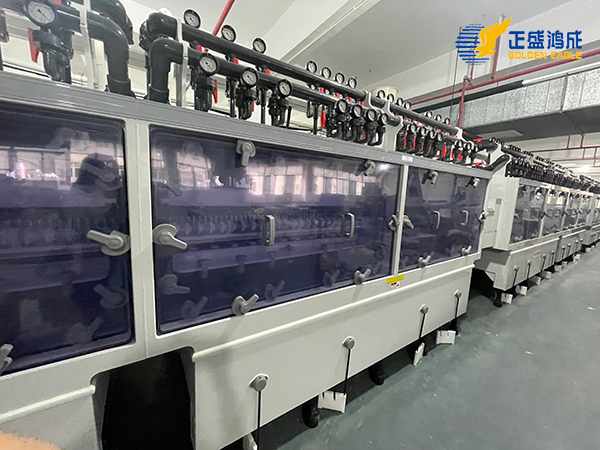
Etching Machine for Lead Frame Manufacturing
A lead frame etching machine is a precision dual-side conveyor etcher for the copper or copper-alloy strips used in IC and LED packaging. The line patterns millions of frames per shift at 50–100 µm line/space, runs half-etching (controlled 30–50 % thickness removal) for die-pad recess, and is followed by electrolytic silver or nickel-palladium-gold plating. Material is typically C194 (Cu-Fe-P) or C7025 (Cu-Ni-Si) at 0.10–0.30 mm thickness. Tolerances are ±10 µm on trace width, ±5 µm on half-etch depth.
A lead frame is the metal carrier that holds a silicon die and connects it to the outside world. It is etched from a thin copper-alloy strip at extremely high precision — 50 to 100 µm line/space, ±10 µm tolerance, on 100 to 300 µm thick material. The etched frame is then plated with silver (for solderable leads) or nickel-palladium-gold (for wire-bondable die pads). The lead frame etching line is one of the most demanding in the electronics industry — the equipment, chemistry, and process control are all precision-grade.
What Is a Lead Frame and How Is It Used?
A lead frame is a thin metal structure with two regions: a central die pad (where the silicon die is glued and wire-bonded) and a surrounding array of leads (which connect the die to the PCB through soldering). The frame is etched from a continuous metal strip, plated, then stamped (or sawed) into individual units. Each unit is loaded into a mold, the silicon die is glued and wire-bonded, and the package is over-molded with epoxy.
Lead frame etching has two distinct patterns:
- Through-etch. The pattern is cut all the way through the strip. This creates the leads, the die-pad outline, and the index holes.
- Half-etch. The pattern is etched to 30 – 50 % of the strip thickness. This creates a recess on the underside of the die pad (or on specific leads) that the molding compound flows into, locking the die in place and preventing die-pad delamination.
Lead Frame Materials
| Alloy | Composition | Tensile strength | Conductivity | Use case |
|---|---|---|---|---|
| C194 (Cu-Fe-P) | Cu-2.3Fe-0.1P-0.1Zn | 400 – 500 MPa | 65 % IACS | QFP, TQFP, SOIC — most common lead-frame alloy |
| C7025 (Cu-Ni-Si) | Cu-3Ni-0.7Si-0.1Mg | 600 – 750 MPa | 40 % IACS | High-lead-count QFN, power packages — high strength |
| Kovar (Fe-Ni-Co) | Fe-29Ni-17Co | 500 – 600 MPa | 4 % IACS | Glass-sealed packages, hermetic — matches glass CTE |
| Cu-OFE (C10100) | 99.99 % Cu | 200 – 250 MPa | 101 % IACS | High-power / RF — not for fine-pitch |
| Cu-C194 + Ag plating | C194 + 3 – 8 µm Ag | Same as C194 | Lead surface — solderable | |
| Cu-C7025 + NiPdAu | C7025 + Ni + Pd + Au | Same as C7025 | Wire-bondable die pad |
Lead Frame Etching Process
Step 1: Strip Cleaning
The incoming strip is degreased in alkaline cleaner (NaOH 5 %, 50 °C) then micro-etched in dilute sulfuric acid / hydrogen peroxide (10 % H₂SO₄ + 3 % H₂O₂, 30 °C) to remove 1–2 µm of surface copper and expose fresh metal. The strip is rinsed in deionized water and dried with hot air. Strip width is 20 – 70 mm (QFP) or 50 – 100 mm (QFN/LQFP), and strip length is 50 – 200 m per reel.
Step 2: Photoresist Lamination
Dry-film photoresist (DFR) at 25 – 38 µm is laminated at 105–115 °C, 2–3 bar, 1–2 m/min. The DFR is slit and punched to match the strip width, with alignment holes that match the strip sprocket holes. Critical: the lamination must be defect-free — any dust, oil, or wrinkle on the strip creates a void in the DFR, which becomes an etch pit in the copper.
Step 3: Exposure
Collimated UV exposure at 50 – 80 mJ/cm². The artwork is a 1:1 glass or film photomask with the lead-frame pattern. Alignment is critical: the mask is registered to the strip sprocket holes using a CCD vision system. Typical alignment accuracy: ±5 µm.
Step 4: Development
1.0 – 1.5 % sodium carbonate at 30 °C, 30–60 seconds. The exposed DFR washes away in the developer, leaving the lead pattern as bare copper with the rest of the strip protected by DFR. Over-development attacks the side wall of the DFR opening and produces tapered lead walls.
Step 5: Etching
Cupric chloride is the standard chemistry for lead-frame etching. Etch rate 25 – 40 µm/min/side at 48 – 52 °C. Etch factor 2.0 – 2.5 (side wall 50 – 60° from vertical). The bath is regenerated continuously with chlorine gas or sodium chlorate, keeping the Cu²⁺/Cu⁺ ratio at 3 – 4 : 1. For half-etching, the conveyor speed is set so the strip is in the chamber for 30 – 50 % of the through-etch time. The half-etch depth is controlled to ±5 µm.
Step 6: Stripping and Cleaning
The remaining DFR is stripped in 3 % NaOH at 50 °C, 60–90 seconds. The strip is then rinsed in cascade DI water and dried with hot air at 80 °C.
Step 7: Plating
Two plating options:
Plating options for lead frame
- Silver (Ag) plating on the leads, 3 – 8 µm thick, for solderable lead finish. Done by electrolytic or immersion plating.
- Nickel-Palladium-Gold (NiPdAu) plating on the die pad, 0.5 – 3 µm Ni + 0.05 – 0.2 µm Pd + 0.05 – 0.1 µm Au, for wire-bondable surface. Done by electrolytic plating in a dedicated reel-to-reel plating line.
- Tin (Sn) plating for lead-free solder, 5 – 15 µm, by hot-dip or electrolytic.
Lead Frame Etching Line Equipment
A lead-frame etching line is configured as a horizontal reel-to-reel conveyor system. The strip runs through 6 – 8 chambers in series, with intermediate rinses between each. Key equipment features:
- Reel-to-reel handling. Pay-off reel, take-up reel, strip accumulator (10 – 30 m) between stages, and a tension dancer for ±0.5 N tension control. Sprocket-driven or capstan-driven transport.
- Conveyor width 20 – 100 mm. Matches the strip width. Spray bars above and below, with adjustable angle (15 – 30° from vertical).
- High-precision etcher chamber. 1.5 – 3.0 m long, with 6 – 12 spray bars per side. PP or PVDF construction. Etch rate uniformity ±5 % across the strip width.
- Online etch-depth monitoring. Laser triangulation or X-ray fluorescence sensor at the chamber exit. Reads the half-etch depth in real time, adjusts conveyor speed via PID loop.
- Dedicated developer and stripper. Spray chambers with soft-spray nozzles. Dwell time controlled by conveyor speed.
- DI water rinse and hot-air dryer. Three-stage cascade rinse. Hot air at 80 – 100 °C. Strip moisture at exit: < 50 ppm.
- Vision inspection before plating. Automated optical inspection (AOI) with line-scan camera. Detects over-etch, under-etch, missing leads, shorts, and contamination.
Half-Etch Process Control
Half-etching is the most critical step in lead frame manufacturing. The half-etch depth must be 30 – 50 % of the strip thickness, with a tolerance of ±5 µm. Too shallow and the molding compound does not lock the die pad; too deep and the die pad is mechanically weak.
Half-etch control
- Half-etch depth = (strip thickness × 0.30 – 0.50) ± 5 µm
- For a 0.20 mm strip, the target is 60 – 100 µm deep
- Control: online laser triangulation sensor reads depth at chamber exit, sends signal to PLC, PLC adjusts conveyor speed (±5 %)
- Bath temperature must be stable to ±1 °C — every 1 °C changes etch rate by 3 – 5 %
- Cu²⁺ concentration must be stable to ±5 g/L — every 10 g/L changes etch rate by 5 – 8 %
Common Lead Frame Etching Defects and How to Prevent Them
| Defect | Cause | Prevention |
|---|---|---|
| Over-etched leads (too thin) | Etch time too long, temperature too high, low Cu²⁺ | Lower conveyor speed; check temperature; check Cu²⁺ hourly |
| Under-etch (leads not separated) | Etch time too short, temperature too low, high Cu²⁺ | Slow conveyor; raise temperature; check Cu²⁺ |
| Tapered lead walls (non-vertical) | Spray not perpendicular, low etch factor | Adjust spray bar angle to 25–30° from vertical; check bath chemistry |
| Half-etch depth out of spec | Bath drift, conveyor speed drift | Online depth sensor with PID control; recalibrate sensor daily |
| Lead shorts (copper bridges) | DFR voids from dust/wrinkles | Clean room DFR lamination; visual inspection of lamination |
| Plating voids on die pad | Residue on copper after etching, poor pre-plate cleaning | Micro-etch before plating; DI water rinse; check Ni strike |
| Die-pad warp after etching | Residual stress in strip; half-etch depth non-uniform | Stress-relief anneal before plating; check half-etch depth uniformity |
Lead Frame Etching Line Specifications
| Spec | R&D / prototype | Production | High-volume |
|---|---|---|---|
| Throughput | 1,000 – 5,000 frames/shift | 20,000 – 100,000 frames/shift | 100,000 – 1,000,000 frames/shift |
| Strip width | 20 – 50 mm | 30 – 80 mm | 50 – 100 mm |
| Min line/space | 75 µm / 75 µm | 50 µm / 50 µm | 50 µm / 50 µm |
| Half-etch depth tolerance | ±10 µm | ±5 µm | ±5 µm |
| Etch chamber length | 1.5 m | 2.5 m | 3.0 m |
| Line speed | 0.5 – 1.5 m/min | 1 – 3 m/min | 2 – 5 m/min |
| Bath volume | 200 L | 600 L | 1,500 L |
| Operator count | 1 / shift | 2 / shift | 2 / shift |