
LED PCB Production Guide
A complete walkthrough of the single-side PCB production line for LED, FR4 and AL CCL boards. The wet-process line is the simplest and most common PCB line in the world — covering 80% of consumer electronics, all LED lighting, and most low-cost industrial control. This guide covers the line layout, the 8 process stages, machine selection, throughput and budget.
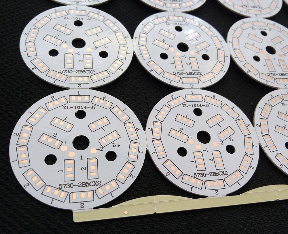
A single-side printed circuit board is the workhorse of LED lighting, consumer electronics, low-cost industrial control, and household appliances. Unlike a double-side or multilayer board, a single-side board is processed only on one side of the substrate — usually FR-4, CEM-1, or aluminium-clad copper laminate (AL CCL) for LED applications. The wet-process line is the simplest PCB line in production, the cheapest to install, and the most common in the world. This guide explains the 8 process stages, the machine selection, and how to size a single-side line for your target output.
A single-side PCB has copper on one side of the substrate only — the other side is bare laminate. There is no plated through-hole, no inner layer, no lamination. The circuit pattern is created by etching the copper on the top side, leaving the substrate untouched. Typical applications: LED lighting (panel lights, downlights, street lights, light strips), consumer electronics (toys, remote controls, calculators, small appliances), industrial control (relay boards, sensor modules, low-power control units), and household appliances. The substrate is usually 0.8–1.6 mm FR-4, with panel sizes from 200×300 mm to 600×1200 mm depending on the throughput target.
A single-side line is significantly simpler than a double-side line. Eight stages cover the full process from raw laminate to a tested, packed, finished board.
FR-4 or AL CCL sheets arrive in 1.0×1.0 m or 1.2×1.0 m panels. A V-cut or shear cutting machine breaks them down to the working panel size. Cutting is the highest-throughput stage and a 0.8–1.0 m wide shear easily handles 200–300 sheets per hour.
Single-side PCBs have through-holes only — no plated holes, no vias. A 3-spindle CNC drilling machine is the workhorse. For LED applications the hole density is low and a 3-spindle machine handles 35,000–60,000 holes per shift. For high-density LED display panels (P1.2–P2.5) the hole count goes up and a 6-spindle machine is recommended.
After cutting and drilling, the panel surface has copper burrs, oxidation, and organic contamination. A deburring-brushing machine removes the burrs and exposes a clean copper surface. For LED applications on AL CCL, brushing is critical because the aluminium side has to be masked off during etching.
Dry-film photoresist is hot-roll laminated onto the copper side. The panel then goes through a UV exposure machine (UV-LED or mercury lamp) with a phototool or, for higher-resolution work, an LDI (Laser Direct Imaging) machine. For most LED and consumer applications a UV-LED exposure machine is sufficient at 50–75 µm line & space.
The unexposed dry-film is dissolved in 1% Na2CO3 solution in a spray developing machine, revealing the copper pattern that will be etched. See our PCB developing machine buying guide for chemistry and process control details.
The exposed copper (not protected by the dry-film) is dissolved in a ferric chloride or alkaline ammonia etching machine. This is the heart of the line. A 650 mm wide conveyor etching machine at 2 m/min produces 25–30 m²/hour of finished single-side board. For AL CCL (LED applications), alkaline ammonia is preferred because it does not attack the aluminium side.
The dry-film is stripped in a 3–5% NaOH solution, then the panel is rinsed and dried. For LED applications the next step is often a solder mask (LPISM, screen-printed) on the copper side, plus a legend print for component identification. These are usually added as part of the same line.
The panel is V-cut or routed into individual boards, electrically tested (continuity test for single-side is much simpler than double-side), and packed. For LED applications the final board is often combined with an aluminium heat-sink or LED lens assembly in a separate line.
LED PCBs are typically made on aluminium-clad copper laminate (AL CCL) rather than FR-4, because the aluminium acts as a heat sink for the LED. The challenge is that the etching chemistry must not attack the aluminium side. This means the line needs alkaline ammonia (NH3-based) etchant, not ferric chloride, because ferric chloride attacks aluminium aggressively. The dry-film lamination also needs to be on the copper side only, with the aluminium side protected by either the laminate carrier film or a spray mask.
For high-brightness LED applications (street lights, automotive headlights, high-power industrial lighting) the copper thickness is often 2–4 oz (70–140 µm) instead of the standard 1 oz (35 µm). This is to carry the higher current. The etching time goes up accordingly — a 2 oz copper takes 18–25 minutes in alkaline ammonia at 50 °C, versus 8–15 minutes for 1 oz.
A standard 12-machine single-side line produces 80–150 m²/month at 2 shifts, or 1,000–1,800 m²/year. This is enough for most LED lighting manufacturers, consumer electronics assembly houses, and small industrial control board producers. For a 500 m²/month LED lighting line, add a second etching machine, a second exposure machine, and a second drilling machine. For a 1,000 m²/month line, the equipment list is roughly the same as a small double-side line (see our double-side PCB production line guide for comparison).
A 12-machine single-side line costs USD 200,000–400,000 ex-works, depending on the level of automation. A fully automatic line with conveyor bridges, robotic loading, and AOI is at the upper end; a semi-automatic line with manual loading is at the lower end. The line fits in 600–800 m² of floor space, runs on three-phase 380 V at 200–300 kVA, and uses 10–20 m³/day of process water. The wastewater is segregated into copper-bearing, alkaline, and general rinse streams. For wastewater handling see our etching wastewater treatment guide.
Choose single-side when: the circuit fits on one copper layer, there are no plated through-holes, the product is price-sensitive (LED lighting, consumer electronics, household appliances), and the monthly volume is below 300 m². Choose double-side when: the circuit needs more than 8–10 components per board, there are plated holes, or the product requires multilayer construction. Most PCB shops start with single-side and add a double-side line within 2–3 years as their customers move up-market.