PCB Etching Process Step by Step: From Design to Finished Board
The PCB etching process is one of the oldest and most standardised manufacturing flows in electronics. The same 8–10 step process that produced the first commercial printed circuit boards in the 1950s still produces most of the world's PCBs today, with each step refined for tighter line / space, smaller vias, and the high yield that modern electronics requires. This guide walks through the complete PCB etching process step by step, from CAD design to finished board.
The PCB etching process is one of the oldest and most standardised manufacturing flows in electronics. The same 8–10 step process that produced the first commercial printed circuit boards in the 1950s still produces most of the world's PCBs today, with each step refined for tighter line / space, smaller vias, and the high yield that modern electronics requires. This guide walks through the complete PCB etching process step by step, from CAD design to finished board.
Quick Answer
- Step 1: CAD design and CAM output — schematic, layout, gerber and drill files.
- Step 2: Substrate preparation — cut blank, drill, plate through-holes, clean.
- Step 3: Photoresist application — dry film laminate or liquid photoresist.
- Step 4: Imaging — UV exposure through a phototool.
- Step 5: Development — dilute Na2CO3 spray to remove unexposed resist.
- Step 6: Etching — cupric chloride or ferric chloride on a conveyorised spray line.
- Step 7: Strip — NaOH to remove the remaining resist.
- Step 8: Finishing — solder mask, surface finish, electrical test, route, score, V-cut.

What Is the PCB Etching Process?
The PCB etching process is the manufacturing flow that turns a digital design into a physical printed circuit board. The basic idea is the same as any photochemical etching:
- Start with a copper-clad laminate (CCL): a sheet of fibreglass (FR-4, CEM, or other substrate) clad with copper on one or both sides.
- Apply a photoresist that covers the copper where the circuit traces should remain.
- Image the photoresist with UV light through a phototool that defines the circuit pattern.
- Develop the resist: the unexposed resist washes away, leaving the copper pattern exposed where the etchant will attack.
- Etch: the exposed copper is dissolved by an etchant, leaving only the protected copper traces.
- Strip the resist and finish the board for soldering.
Each step has variations depending on the type of board (single-sided, double-sided, multilayer), the line / space of the design, and the end application. The standard PCB etching process is the same on the inside; the equipment and chemistry scale with the board complexity.
Step 1: CAD Design and CAM Output
The PCB etching process starts with the design. The engineer creates the schematic and the layout in a CAD tool (Altium Designer, KiCad, OrCAD, EAGLE, etc.), and the output is a set of files:
- Gerber files. The standard format for PCB manufacturing. One Gerber per layer — top copper, bottom copper, top solder mask, bottom solder mask, top silkscreen, bottom silkscreen, and the board outline.
- Drill files. Excellon format, listing every through-hole and via with its X-Y position and drill size.
- Stack-up definition. For multilayer boards, the order and thickness of each layer.
- Netlist. For electrical test, the expected connectivity of every net.
The CAM engineer at the PCB fab verifies the files, runs design rule checks, and generates the phototools for the imaging step.
Step 2: Substrate Preparation
The substrate is a copper-clad laminate (CCL) cut to the panel size. For through-hole boards, the next steps are drilling and plating; for single-sided boards, drilling and plating can be skipped or done later.
Cutting and cleaning
The CCL sheet is cut to the working panel size (typically 18×24 inch or similar). The cut panels are brushed and cleaned to remove surface contamination.
Drilling
A CNC drill hits the panel with the drill program from the CAM output. Through-holes, vias, and mounting holes are all drilled at this stage. The drill hits are referenced to a precise origin on the panel, and the drill file includes all the alignment targets for the imaging step.
Through-hole plating
For double-sided and multilayer boards, the through-holes are plated with copper to make them conductive. The standard process is electroless copper (a thin, uniform copper layer is deposited on the hole walls without electricity), followed by electroplating to build up the thickness to about 25 µm.
Surface preparation
The copper surface is cleaned and micro-etched to give the photoresist good adhesion. The cleaning is usually a pumice scrub, an alkaline clean, and a micro-etch with dilute sulfuric acid or sodium persulfate.
Step 3: Photoresist Application
The photoresist is what protects the copper traces during etching. Two main types:
Dry film
A dry-film photoresist is a three-layer laminate (cover sheet, photoresist, base sheet) that is hot-roll laminated onto the copper surface. The roll laminator applies heat and pressure, the cover sheet is peeled off, and the photoresist is exposed on the copper. Dry film is the standard for through-hole and multilayer PCB work.
Liquid photoresist
A liquid photoresist is a photoimageable solder mask ink (such as YB-800) that is screen-printed, spray-coated, or curtain-coated onto the copper. Liquid photoresist is the standard for fine-line SMT work, where the thinner coating gives better resolution than dry film.
For a PCB etching line, the choice between dry film and liquid resist is a process decision. Most production lines use dry film for the etch resist and liquid resist (solder mask) for the final solder mask. Some fine-line lines use liquid resist for both.
Step 4: Imaging
The panel is exposed to UV light through a phototool. The phototool is a high-resolution film with the circuit pattern printed in black on a clear background. The UV light cross-links the exposed photoresist; the unexposed resist remains soluble.
For double-sided boards, the panel is exposed on both sides in a single operation, with the top and bottom phototools aligned to the drill origin. For multilayer boards, the inner layers are imaged, developed, etched, and laminated into a stack before the outer layers are imaged.
Step 5: Development
The panel is sprayed with dilute sodium carbonate (Na2CO3, typically 0.8–1.2% by weight) at 30 °C, with spray pressure around 2 kg/cm². The unexposed resist washes away, leaving the copper pattern exposed where the etchant will attack.
The development step is the most critical step for line / space control. The development time, temperature, and pressure must be tightly controlled; under-development leaves resist in the etched areas, over-development attacks the sidewall of the resist and gives ragged edges.
Step 6: Etching
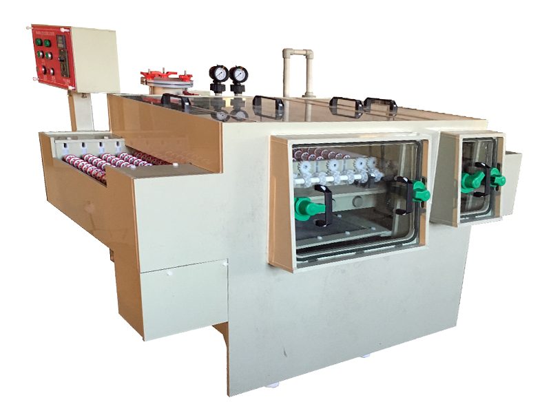
The developed panel is run through a PCB etching machine on a conveyorised spray line. The etchant attacks the exposed copper and dissolves it; the protected copper traces remain. The standard PCB etchants:
- Cupric chloride (CuCl2). The standard etchant for production PCB work. Fast, regenerable, vertical sidewall. Etch rate typically 35–50 µm/min.
- Ferric chloride (FeCl3). The traditional etchant. Slower than cupric chloride, but easier to run. Etch rate typically 25–40 µm/min.
- Alkaline ammonia. Used for inner layers of multilayer boards where the chemistry must not attack the laminate. Slower etch rate, requires tight control.
The etching machine has a regeneration system that doses the bath with oxidant (chlorine gas, hydrogen peroxide, or sodium chlorite for cupric chloride) and water to keep the etch rate constant. The conveyor speed is set so the etch time is just enough to remove the required copper thickness.
Key parameters during etching
- Etchant temperature. 45–55 °C for both cupric chloride and ferric chloride. Higher temperature = faster etch, but more fume and more rapid bath degradation.
- Etchant concentration. Specific gravity 1.36–1.46 for ferric chloride; ORP 400–500 mV for cupric chloride.
- Spray pressure. 1–3 bar at the nozzles. Even coverage is critical; a dead stripe gives a panel with under-etched copper.
- Conveyor speed. Set to give the correct etch time. Typical 0.5–2 m/min on a 600 mm line.
Step 7: Strip
The remaining photoresist is stripped in a sodium hydroxide (NaOH) bath, typically 10% by weight at 50–80 °C. The resist dissolves and the bare copper traces are exposed. The panel is then rinsed and dried.
Step 8: Finishing
After etch and strip, the PCB goes through several finishing steps before it is ready for component assembly:
- Solder mask. A liquid photoimageable solder mask (such as YB-800) is applied to the entire board except the pads and vias. The board is exposed, developed, and cured. Solder mask gives the green (or other colour) coating on the finished board.
- Surface finish. The exposed copper pads are coated with a finish to prevent oxidation and improve solderability. Common finishes: HASL (hot air solder leveling), ENIG (electroless nickel / immersion gold), OSP (organic solderability preservative), immersion tin, immersion silver.
- Silkscreen. Component reference designators and other markings are printed on the board in white ink.
- Electrical test. Every net is tested for continuity and isolation. Failures are marked for repair.
- Route and score. The panel is cut into individual boards using a CNC router, a V-cut scoring machine, or a punch.
Variations on the Process
Single-sided PCB
Single-sided PCBs skip the through-hole plating step. The board has copper on one side only, no through-holes, and the etching removes the unwanted copper from the one copper side. The rest of the process is the same.
Double-sided PCB
Double-sided PCBs have copper on both sides, with through-holes connecting the two sides. The plating step is required to make the through-holes conductive. The imaging step exposes both sides in a single operation with the two phototools aligned to the drill origin.
Multilayer PCB
Multilayer PCBs have 4, 6, 8, or more copper layers sandwiched between prepreg and core materials. The inner layers are imaged, developed, etched, and oxidised, then laminated into a stack with the outer layers. The outer layers are then imaged, developed, and etched. The process is more complex but the chemistry is the same.
Flexible PCB
Flexible PCBs use a polyimide film instead of FR-4. The chemistry is the same as for rigid PCB, but the substrate is thin and flexible, requiring careful handling through the etching line.
Common Defects and How to Avoid Them
| Defect | What it looks like | Most common cause |
|---|---|---|
| Under-etch | Copper bridges between traces | Conveyor too fast, etchant temperature dropped, etchant exhausted |
| Over-etch | Traces too thin, breaks in fine lines | Conveyor too slow, etchant too hot or too concentrated |
| Undercut | Traces narrower than artwork | Etchant too aggressive, etch time too long, no sidewall protection |
| Resist residue | Copper residue between traces | Under-development, resist not fully cured, etch breakthrough under resist |
| Mis-registration | Traces off-centre from pads / holes | Phototool alignment error, panel movement through the line |
| Etch pitting | Pits in the copper surface | Bath contamination, poor filtration, gas bubbles in spray |
Most of these defects are caught at the AOI (automated optical inspection) step before the board goes to surface finish. The standard target yield for a well-tuned PCB etching line is 95–99%.
Setting Up a PCB Etching Line?
Send us your largest panel, your minimum line / space, your copper weight, your monthly volume and the chemistry you prefer. Golden Eagle will configure a PCB etching line with regeneration, AOI, surface finish and stack-up to match.
Configure a LineConclusion
The PCB etching process is an 8-step flow from CAD to finished board: design and CAM, substrate preparation, photoresist application, imaging, development, etching, strip, and finishing. Each step has its own equipment and chemistry, but the basic idea — mask the copper, etch the unmasked, strip the mask — has not changed in 70 years. With a well-tuned conveyorised etching line, a regeneration system, and proper AOI, the process runs at 95–99% yield and produces the high-density, fine-line PCBs that modern electronics requires.