
What Is Photochemical Etching? Process, Materials & Applications
Photochemical etching is a precision metal-fabrication process that uses light-sensitive masking and a chemical etchant to dissolve unwanted metal and leave behind a finished part. It is also known as photochemical machining (PCM), photo etching, or chemical etching. Because the process removes metal with chemistry rather than mechanical force or heat, it produces flat, burr-free, stress-free parts with very fine detail — and it does so without the expensive hard tooling that stamping requires.
This guide explains what photochemical etching is, how the process works step by step, which metals can be etched, the tolerances you can expect, and how PCM compares with stamping, laser cutting, and CNC machining.
Quick Answer
- Photochemical etching (PCM) is a manufacturing process that uses a photoresist mask and a chemical etchant to selectively dissolve metal and form a precise part.
- It works on most engineering metals — stainless steel, copper, brass, nickel, aluminium, and even titanium.
- Parts are burr-free and stress-free, with no hardening of the metal and no costly hard tooling.
- Typical tolerances are about ±10% of the metal thickness, holding fine features down to roughly 0.1 mm.
What Is Photochemical Etching (PCM)?
Photochemical etching combines two technologies: photolithography (transferring an image onto a surface using light) and chemical etching (dissolving metal with an acidic etchant). A digital part design is printed onto a transparent film called a phototool. That image is transferred to a metal sheet coated with a light-sensitive photoresist. After developing, the photoresist protects the areas that should remain, while the exposed metal is etched away.
The result is the same family of work covered in our overview of the chemical etching process, but with the defining feature that the pattern is created photographically. This makes PCM ideal for parts with complex, repeating, or very fine features — from precision shims and lead frames to filter meshes, encoder discs, and decorative panels.

How Does the Photochemical Etching Process Work?
The photochemical etching process follows the same core sequence whether you are making circuit boards or precision metal parts. Each stage runs on dedicated equipment, and consistency at every step is what delivers a clean, repeatable result.
- Cleaning. The metal sheet is chemically cleaned and scrubbed to remove oils, oxides, and contamination so the photoresist bonds evenly across the surface.
- Photoresist coating / lamination. A light-sensitive film (dry-film photoresist) is laminated to both sides of the metal, or a liquid resist is coated and dried.
- UV exposure. The phototool carrying the part image is placed over the metal and exposed to UV light, which hardens the resist in the image areas. Double-sided parts are exposed on both faces in precise registration.
- Developing. A developer solution washes away the unhardened resist, uncovering the bare metal that will be etched.
- Etching. The sheet passes through a spray etching machine where a heated etchant — usually ferric chloride — is sprayed under pressure to dissolve the exposed metal cleanly and evenly.
- Resist stripping. The remaining photoresist is chemically stripped, leaving the finished bare-metal part.
- Rinsing & inspection. Parts are rinsed, dried, and inspected for dimensional accuracy and edge quality.
For a deeper look at the chemistry and at how the same steps are applied to circuit boards, see our article on the PCB etching process.
What Metals Can Be Photochemically Etched?
One of the biggest advantages of PCM is its material flexibility. Because the etchant — not a hardened die — does the cutting, switching alloys often means only changing the chemistry and timing, not buying new tooling. Commonly etched metals include:
- Stainless steel (301, 304, 316, 430 and more) — the most widely etched metal. See our guide to stainless steel etching.
- Copper and copper alloys — brass, bronze, beryllium copper, and phosphor bronze, used for connectors, shims, and lead frames.
- Nickel and nickel alloys — including nickel-silver and Inconel for masks and aerospace parts.
- Aluminium — for lightweight shields, nameplates, and heat-spreaders.
- Titanium — for medical, aerospace, and foldable-phone parts (see our dedicated guide to titanium etching).
- Specialty alloys — molybdenum, Kovar, Invar, and spring steels used in electronics and precision instruments.
Tolerances and Capabilities
Photochemical etching is a thin-metal process. It is best suited to foil and sheet from roughly 0.01 mm to 2 mm thick. As a general rule, the achievable tolerance scales with thickness — typically about ±10% of the metal thickness — so thinner material holds tighter detail. On thin stock, edge features down to around 0.1 mm and tolerances near ±0.025 mm are realistic. Because etching attacks the metal from the side as well as downward (an effect called undercut), well-controlled spray pressure, temperature, and conveyor speed are essential to hold these figures.
Photochemical Etching vs Stamping, Laser & CNC
PCM is not the right answer for every part, but it has clear strengths for thin, detailed, flat components — especially at prototype to medium volumes where hard tooling is hard to justify.
| Factor | Photochemical Etching | Stamping | Laser Cutting | CNC Machining |
|---|---|---|---|---|
| Tooling cost | Very low (a photo film) | Very high (hard die) | None | Low–medium |
| Lead time for first parts | Days | Weeks (tooling) | Days | Days |
| Burrs & stress | None — burr-free, stress-free | Burrs, work hardening | Heat-affected edge | Burrs, some stress |
| Cost of complex shapes | No extra cost | Raises tooling cost | Slower per part | Raises machining time |
| Design changes | Cheap & fast (new film) | Expensive (new die) | Easy | Easy |
| Ideal material thickness | ~0.01–2 mm | Wide range | Medium–thick | Any |
| Best volume | Prototype to high volume | Very high volume | Low–medium | Low–medium |
If your decision is specifically between etching and a beam-based process, our comparison of etching vs laser engraving covers the trade-offs in more detail. For parts that need controlled depth rather than a through-cut, see chemical milling.
Key Advantages of Photochemical Etching
- No mechanical stress or burrs — parts stay perfectly flat and need no deburring.
- No heat-affected zone — the metal's hardness, grain, and magnetic properties are unchanged.
- Low-cost, fast tooling — the phototool is inexpensive and can be revised in hours, making it ideal for prototyping.
- Complexity is free — intricate, repeating, or multi-feature patterns cost no more than simple ones.
- Many parts at once — a full sheet of identical or mixed parts is etched in a single pass.
Applications and Industries
Photochemical etching serves almost every precision industry. Typical parts include lead frames and connectors for electronics, fuel-cell bipolar plates and shims for energy, fine filters and meshes for filtration, encoder discs and flexures for instruments, surgical components for medical devices, and decorative panels, etched plaques, and metal nameplates for signage. The same technology underpins metal etching for stainless steel and copper across these markets.
The Equipment Behind the Process
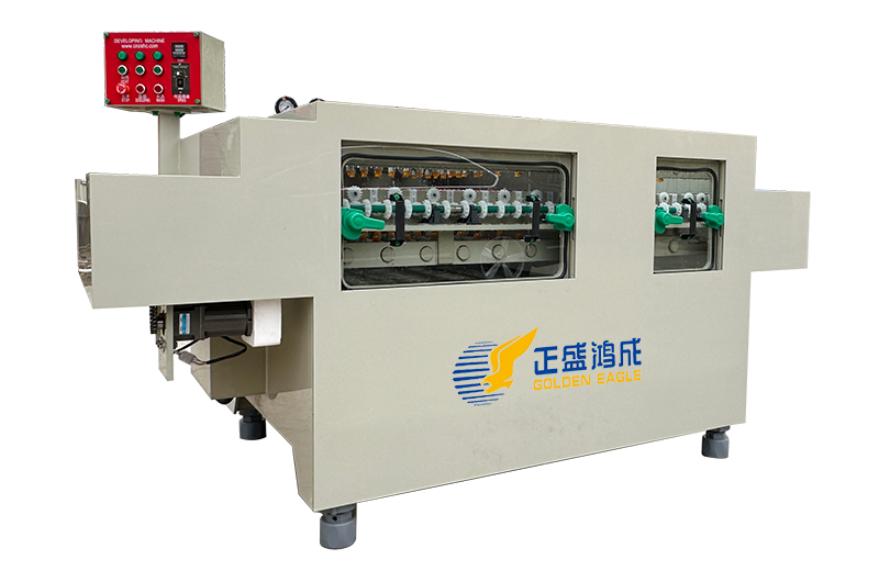
The quality of a photochemically etched part depends as much on the machine as on the chemistry. A production line typically includes a cleaning/brushing machine, a laminator and exposure unit, a developing machine, and — at its heart — a spray etching machine that keeps spray pressure, etchant temperature, and conveyor speed under tight control. For high-detail work, a high-precision etching machine and the correct etching chemicals make the difference between a usable part and a scrapped one. Golden Eagle has built this equipment for the etching industry since 2002.
Planning a Photochemical Etching Line?
Tell us your material, part size, and volume — Golden Eagle will recommend the right etching machine and chemistry for your application.
Talk to an EngineerConclusion
Photochemical etching turns a sheet of metal and a photographic image into precise, burr-free, stress-free parts — without the cost and lead time of hard tooling. Its material flexibility, fine detail, and low tooling cost make it the preferred process for thin, complex components in electronics, medical, energy, filtration, and decorative applications. Match your metal and volume to the right etching equipment, and PCM delivers clean, repeatable results from the first prototype to full production.